Non-volatile semiconductor memory device and manufacturing method thereof

a non-volatile, memory device technology, applied in the direction of semiconductor devices, basic electric elements, electrical appliances, etc., can solve the problems of increasing manufacturing costs, difficult to sufficiently boost such a reduced power supply voltage, complex process of forming capacitors, etc., to achieve the effect of reducing the size and voltage of a non-volatile semiconductor memory device and increasing manufacturing costs

Inactive Publication Date: 2006-03-28
PANASONIC CORP
View PDF5 Cites 9 Cited by
  • Summary
  • Abstract
  • Description
  • Claims
  • Application Information

AI Technical Summary

Benefits of technology

[0008]The present invention is made to solve the above problems, and it is an object of the present invention to obtain a capacitor of a booster which enables reduction in size and voltage of a non-volatile semiconductor memory device without increasing manufacturing costs.

Problems solved by technology

For the conventional non-volatile semiconductor memory device, however, it is difficult to sufficiently boost such a reduced power supply voltage.
However, using a special insulating film in the capacitor alone would make the process of forming the capacitor more complex than the process of forming a storage element, a logic element and the like.
Therefore, it is difficult from the standpoint of manufacturing costs to use such a special capacitance insulating film.
Moreover, increasing the area of the capacitor would impede reduction in size of the non-volatile semiconductor memory device.
As described above, in the conventional non-volatile semiconductor memory device, it is difficult to obtain a capacitor of a booster which enables reduction in size and voltage.

Method used


Image

  • Non-volatile semiconductor memory device and manufacturing method thereof
  • Non-volatile semiconductor memory device and manufacturing method thereof
  • Non-volatile semiconductor memory device and manufacturing method thereof

Examples


first embodiment

[0105](First Embodiment)

[0106]Hereinafter, the first embodiment of the present invention will be described with reference to the accompanying drawings.

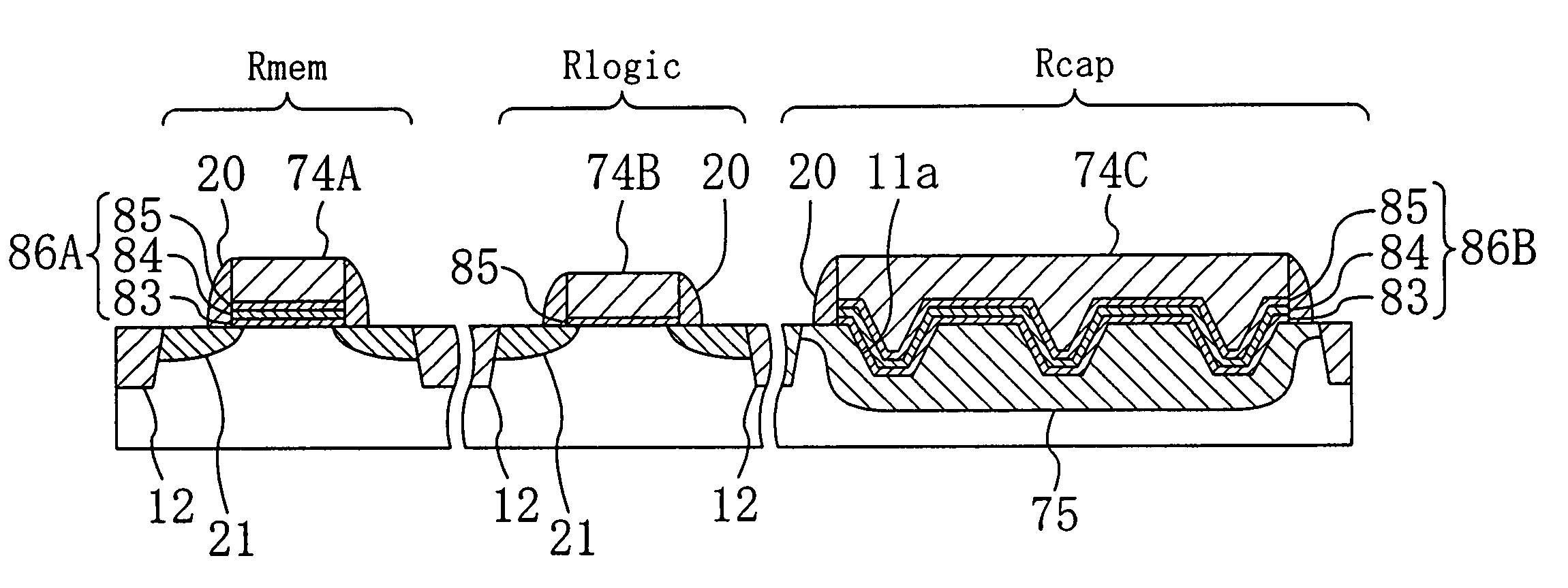
[0107]FIG. 1 shows a cross-sectional structure of a non-volatile semiconductor memory device according to the first embodiment of the present invention. As shown in FIG. 1, an element isolation insulating film 12 is selectively formed in the upper portion of a semiconductor substrate 11. The semiconductor substrate 11 is formed from silicon, and the element isolation insulating film 12 is formed from silicon oxide. Such selective formation of the element isolation insulating film 12 defines a storage circuit region Rmem, a logic circuit region Rlogic, and a capacitor region Rcap. The storage circuit region Rmem is a region including a storage element. The logic circuit region Rlogic is a region including a peripheral circuit or a logic element such as a logic circuit. The capacitor region Rcap is a region including a capacitor of a bo...

second embodiment

[0156](Second Embodiment)

[0157]Hereinafter, the second embodiment of the present invention will be described with reference to the figures.

[0158]FIG. 11 shows a cross-sectional structure of a non-volatile semiconductor memory device according to the second embodiment of the present invention. In FIG. 11, the same members as those of the non-volatile semiconductor memory device of FIG. 1 are denoted with the same reference numerals and characters, and description thereof is omitted.

[0159]As shown in FIG. 11, in the non-volatile semiconductor memory device of the second embodiment, the storage element in the storage circuit region Rmem is formed as a so-called MNOS (Metal Nitride Oxide Semiconductor) type storage element for storing charges in a laminated film of an oxide film and a nitride film.

[0160]An element isolation insulating film 12 is selectively formed in the upper portion of a semiconductor substrate 11 in order to define a storage circuit region Rmem, a logic circuit regio...

third embodiment

[0179](Third Embodiment)

[0180]Hereinafter, the third embodiment of the present invention will be described with reference to the figures.

[0181]FIG. 13 shows a cross-sectional structure of a non-volatile semiconductor memory device according to the third embodiment of the present invention. In FIG. 13, the same members as those of the non-volatile semiconductor memory device of FIG. 11 are denoted with the same reference numerals and characters, and description thereof is omitted.

[0182]As shown in FIG. 13, in the non-volatile semiconductor memory device of the third embodiment, the storage element in the storage circuit region Rmem is formed as an MNOS-type storage element. The non-volatile semiconductor memory device of the third embodiment is different from that of the second embodiment in the structure of the insulating film for storing charges.

[0183]In the storage circuit region Rmem, a charge storage film 73A is formed on a semiconductor substrate 11. The charge storage film 73A...


PUM


Abstract

The non-volatile semiconductor memory device has a booster including a capacitor, and a storage circuit including a storage element. The capacitor has a lower electrode, a capacitor capacitance insulating film and an upper electrode. The lower electrode of the capacitor is shaped to have an increased surface area.

Description

[0001]This application is a divisional of application Ser. No. 10 / 281,176 filed Oct. 28, 2002 now abandoned.BACKGROUND OF THE INVENTION[0002]The present invention generally relates to a non-volatile semiconductor memory device. More particularly, the present invention relates to a non-volatile semiconductor memory device having a booster including a capacitor.[0003]Electrically writable and erasable non-volatile semiconductor memory devices such as flash memory devices and EEPROM (Electrically Erasable and Programmable Read Only Memory) devices use two different voltages, one for read operation and one for write and erase operations. For example, a power supply voltage of 5 V is used for read operation, and a voltage of 12 V, i.e., the power supply voltage boosted by a booster, is used for write and erase operations.[0004]In a conventional non-volatile semiconductor memory device, a booster is formed by booster cells connected in parallel. Each booster cell is formed by a switching ...

Claims


Application Information

Patent Timeline
Patent Type & Authority Patents(United States)
IPC IPC(8): H01L21/8247H01L21/8246
CPCH01L27/11526H01L27/11568H01L27/11534H10B41/43H10B41/40H10B43/30
Inventor TAMURA, NOBUYUKI
Owner PANASONIC CORP
Why Eureka
Try Eureka