Plasma display panel having sealing structure

a technology of plasma display panel and sealing structure, which is applied in the manufacture of electrode systems, electric discharge tubes/lamps, and address electrodes, etc., can solve the problem that the discharge space cannot be kept gas-tightly sealed

Inactive Publication Date: 2006-03-28
FUJITSU HITACHI PLASMA DISPLAY LTD
View PDF6 Cites 10 Cited by
  • Summary
  • Abstract
  • Description
  • Claims
  • Application Information

AI Technical Summary

Benefits of technology

[0014]In accordance with the present invention, there is provided an AC plasma display panel, which comprises: a pair of panels disposed in spaced opposed relation, and each having a plurality of electrodes formed on an opposed surface thereof and mostly covered with a dielectric layer; and a sealing member which seals the periphery of the pair of panels; wherein the electrodes each have a portion uncovered with the dielectric layer, and the sealing member is disposed in contact with the uncovered portions of the electrodes. In the present invention, the electrodes are each partly uncovered with the dielectric layer, and the sealing member directly contacts the uncovered portions of the electrodes. Therefore, no voids are present on the opposite sides and surfaces of the electrodes, so that a discharge space defined between the panels can be kept gas-tightly sealed by the sealing member without communication with the outside of the display panel which may otherwise occur due to the presence of voids on the opposite sides and surfaces of the electrodes. Thus, the plasma display panel can ensure proper display by stable electric discharge for a long period of time.
[0015]In the inventive plasma display panel, the dielectric layer has a cut-away portion formed in a peripheral region thereof, and the sealing member contacts the uncovered portions of the electrodes via the cut-away portion of the dielectric layer. In this case, the cut-away portion is not formed on the peripheral edge of the dielectric layer but in the peripheral region of the dielectric layer, and the sealing member directly contacts the uncovered portions of the electrodes. Therefore, the discharge space can be kept gas-tightly sealed by the scaling member, and portions of the dielectric layer located on longitudinally opposite ends of the electrodes can easily be etched.

Problems solved by technology

Therefore, the discharge space cannot be kept gas-tightly sealed.

Method used


Image

  • Plasma display panel having sealing structure
  • Plasma display panel having sealing structure
  • Plasma display panel having sealing structure

Examples


first embodiment

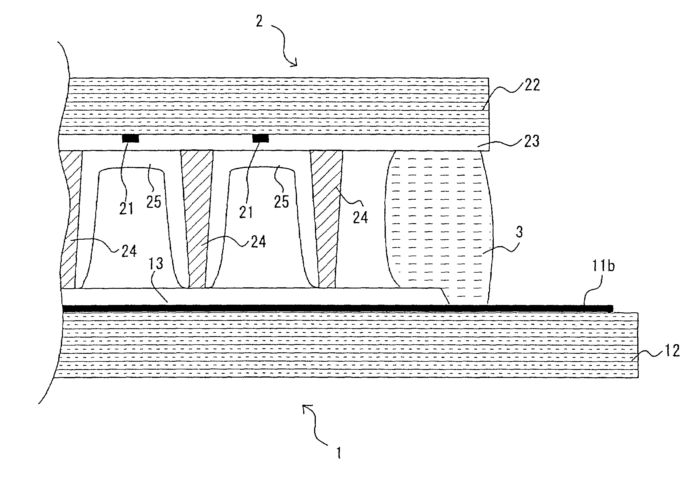
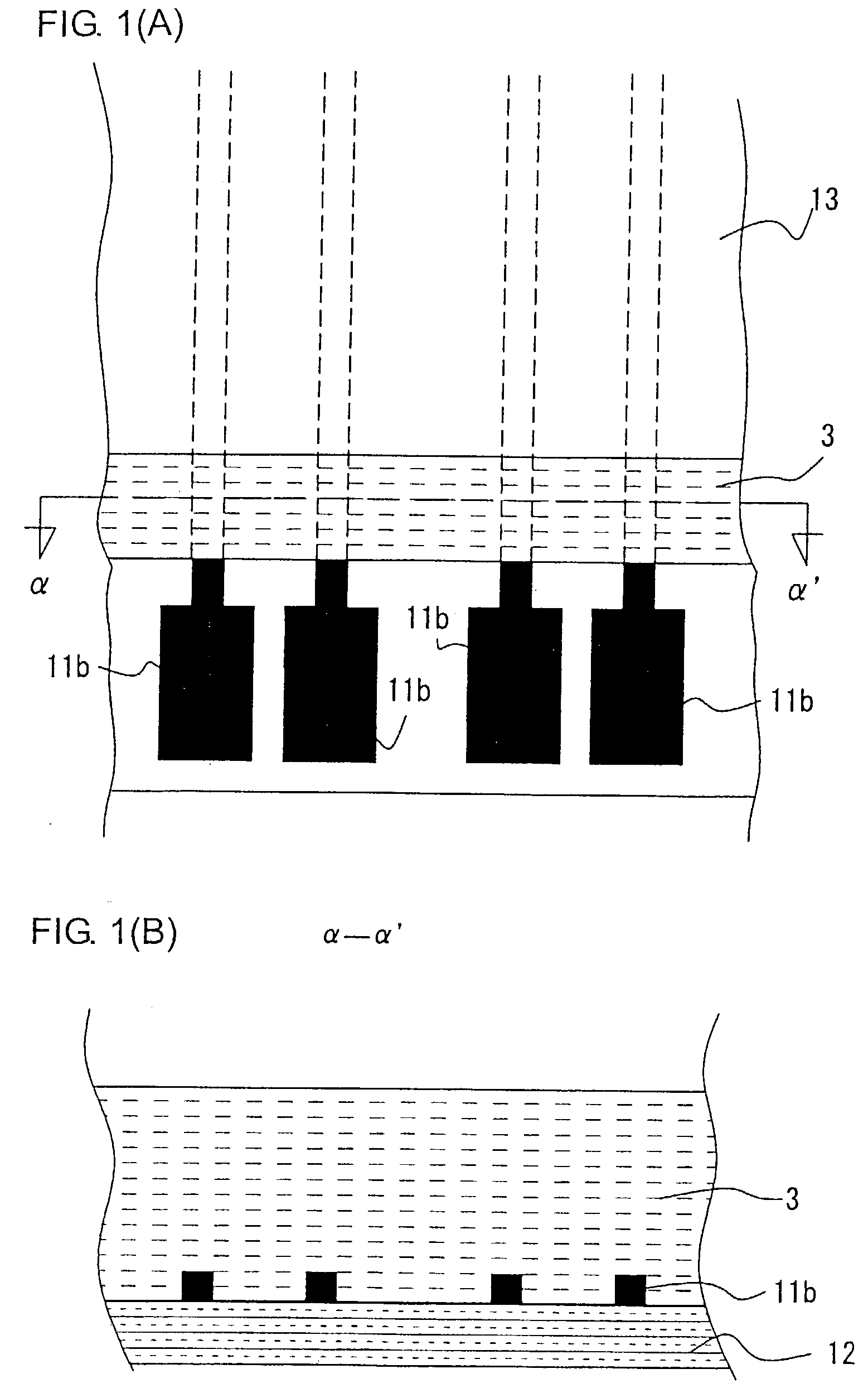
[0026]A plasma display panel according to a first embodiment of the present invention will hereinafter be described with reference to FIGS. 1(A), 1(B) and 2. FIGS. 1(A) and 1(B) are a top view and a sectional view, respectively, illustrating major portions of a front panel of the plasma display panel according to this embodiment, and FIG. 2 is a sectional view illustrating major portions of the plasma display panel according to this embodiment.

[0027]As shown, the plasma display panel according to this embodiment includes a front panel 1 having pairs of main electrodes 11 for display discharge, and a rear panel 2 having address electrodes 21 for address discharge, like the conventional plasma display panel. The front panel 1 and the rear panel 2 are disposed in spaced opposed relation, and a sealing glass member 3 is provided between the front panel 1 and the rear panel 2 in direct contact with the electrodes without intervention of a dielectric layer 13 to define a sealed discharge ...

second embodiment

[0040]Although the plasma display panel according to the first embodiment is constructed such that the opposite end portions of the bus electrodes 11b are not covered with the dielectric layer 13 and the sealing glass member 3 is provided in direct contact with the opposite end portions of the bus electrodes 11b, a plasma display panel according to a second embodiment of the present invention is constructed such that apertures β are formed in the dielectric layer 13 to partly expose the opposite end portions of the bus electrodes 11b and the sealing glass member 3 is provided as filling the apertures β as shown in FIGS. 3(B) and 4. Thus, the sealing glass member 3 is disposed on the opposite end portions of the bus electrodes 11b, and portions 13′ of the dielectric layer 13 are still present on the opposite end portions of the bus electrodes 11b. Therefore, the discharge space can be kept gas-tightly sealed by the sealing glass member 3, and the dielectric layer portions 13′ dispose...

example 1

[0043]Cr, Cu and Cr films were formed on a front panel 1 by the sputtering method, and patterned for formation of bus electrodes 11b. Then, SiO2 was deposited to a thickness of 5.0 μm over the bus electrodes 11b under the following conditions by the plasma CVD method by means of a plasma CVD device of parallel plate type to form a dielectric layer 13 in a region as shown in FIG. 2. Subsequently, MgO was deposited to a thickness of 1.0 μm on the dielectric layer 13 by the vapor deposition method to form a protective film 14.

[0044]

Introduced gas and flow rate:SiH4 / 900 sccmIntroduced gas and flow rate:N2O / 9000 sccmRadio frequency output:2.0 kWSubstrate temperature:400° C.Vacuum degree:3.0 Torr

[0045]Then, a glass paste having a softening point of 430° C. was applied in a region of a sealing glass member 3 as shown in FIG. 2 by the dispenser method, and baked at 500° C. The front panel 1 and a rear panel 2 were baked at 450° C. to be combined in opposed relation. Then, a discharge space ...


PUM


Abstract

An AC plasma display panel has a pair of panels disposed in spaced opposed relation, and each having a plurality of electrodes formed on an opposed surface thereof and mostly covered with a dielectric layer; and a sealing member which seals the periphery of the pair of panels. The electrodes each has a portion uncovered with the dielectric layer, and the sealing member is disposed in contact with the uncovered portions of the electrodes. With this arrangement, the discharge space can be kept gas-tightly sealed by the sealing member without communication with the outside of the display panel which may otherwise occur due to the presence of voids on opposite sides and surfaces of the electrodes.

Description

CROSS-REFERENCE TO RELATED APPLICATION[0001]This application is related to Japanese patent application No. 2002-133997 filed on May 9, 2002, whose priority is claimed under 35 USC § 119, the disclosure of which is incorporated by reference in its entirety.BACKGROUND OF THE INVENTION[0002]1. Field of the Invention[0003]The present invention relates to a plasma display panel and, more particularly, to an AC plasma display panel having a sealing structure for isolating a discharge space from an external environment.[0004]2. Description of the Related Art[0005]A conventional AC plasma display panel will be described with reference to FIGS. 6 to 8. FIG. 6 is a partial perspective view illustrating a plasma display panel of triode surface discharge type known as a typical AC panel, and FIGS. 7(A) and 7(B) are a top view and a sectional view, respectively, illustrating major portions of a front panel of the plasma display panel. FIG. 8 is a sectional view illustrating major portions of the...

Claims


Application Information

Patent Timeline
Patent Type & Authority Patents(United States)
IPC IPC(8): H01J17/49H01J11/22H01J11/12H01J11/24H01J11/26H01J11/38H01J11/46H01J11/48H01J17/18
CPCH01J11/12H01J11/48H01J11/46H01J11/22H01J11/38
Inventor HARADA, HIDEKI
Owner FUJITSU HITACHI PLASMA DISPLAY LTD
Why Eureka
Try Eureka