Method of fabricating a polysilicon thin film

a thin film, polysilicon technology, applied in the direction of vacuum evaporation coating, chemical vapor deposition coating, coating, etc., can solve the problems of difficult control, adversely affecting the tft device, poor crystallization, etc., to reduce the amount and the density of protrusions and smooth the polysilicon thin film

Active Publication Date: 2006-04-04
AU OPTRONICS CORP
View PDF7 Cites 7 Cited by
  • Summary
  • Abstract
  • Description
  • Claims
  • Application Information

AI Technical Summary

Benefits of technology

[0011]An object of the present invention is to provide a method of fabricating a polysilicon thin film for forming a bigger silicon grain and reducing the amount and the density of the protrusions in order to achieve a smoother polysilicon thin film for the TFT devices.

Problems solved by technology

Solid phase crystallization requires high temperatures (600° C.) and the result of the crystallization is not very good.
The power density of each pulse would be different and thus is difficult to control.
As a result, the size of silicon grains left would be different; the silicon grains would comprise protrusions at their boundaries reflecting a poor smoothness of the polysilicon thin film, which would adversely affect the TFT devices.

Method used


Image

  • Method of fabricating a polysilicon thin film
  • Method of fabricating a polysilicon thin film
  • Method of fabricating a polysilicon thin film

Examples


first embodiment

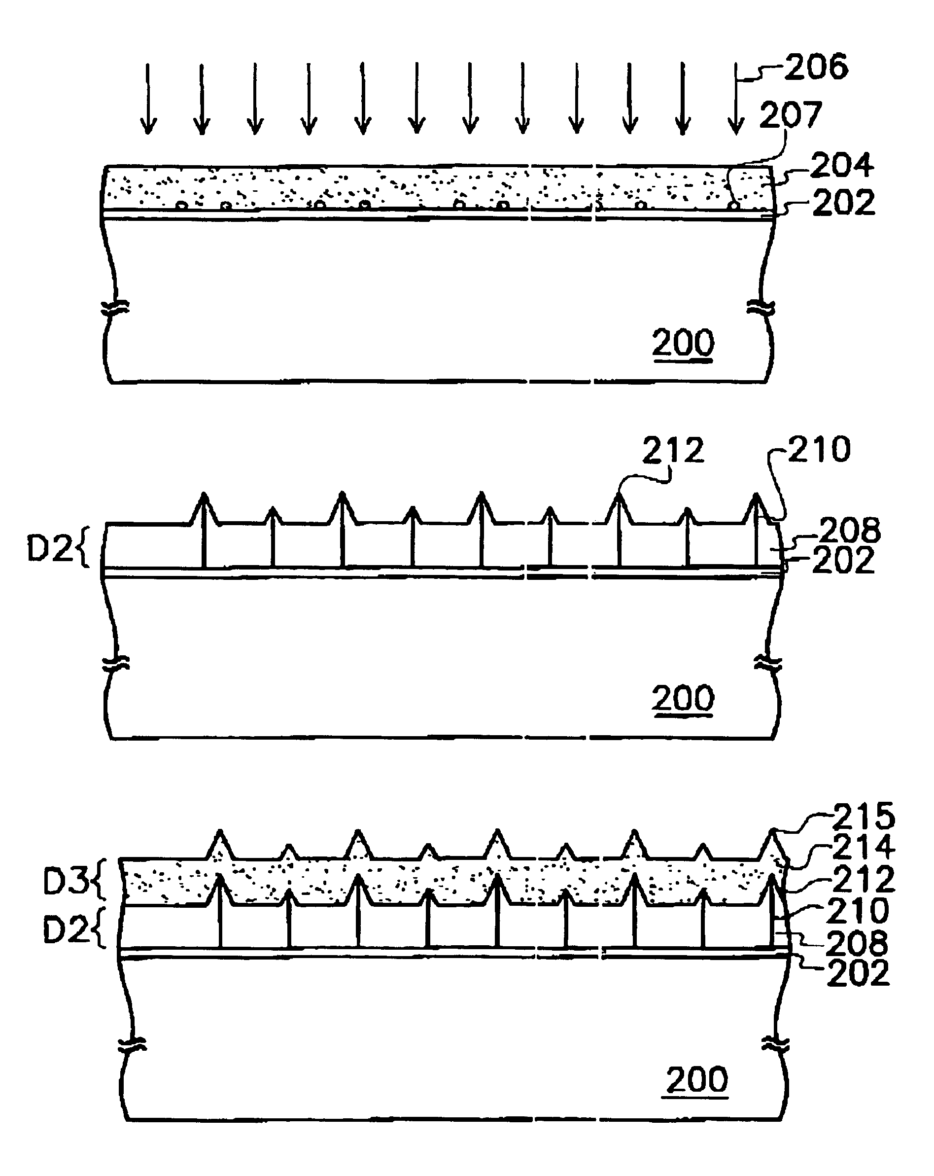
[0020]FIGS. 2A-2F are the cross-sectional views of the process of fabricating a polysilicon thin film in accordance with the present invention.

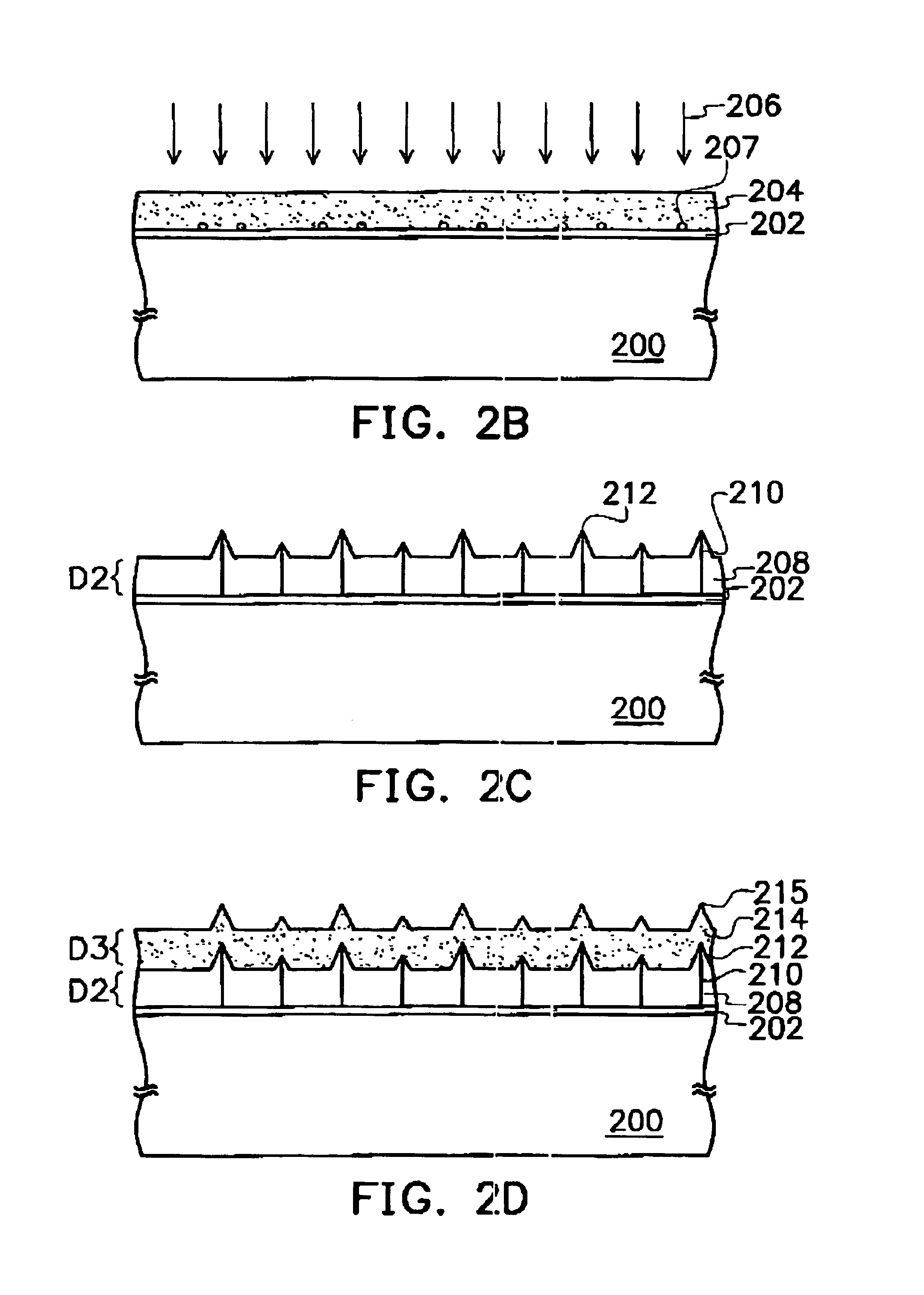
[0021]Referring to FIG. 2A, a substrate 200 is provided; the substrate 200 can be a silicon substrate, a glass substrate or a plastic substrate. Then an isolating layer 202 is formed on the substrate 200; the isolating layer material may include silicon dioxide. The isolating layer 202 can be formed by a low pressure chemical vapor deposition (“LPCVD”), a plasma enhanced chemical vapor deposition (“PECVD”) or a sputter. Next, an amorphous silicon layer 204 is formed on the isolating layer 202; the amorphous silicon layer 204 can be formed by a LPCVD, a PECVD or a sputter, wherein amorphous silicon layer 204 has a thickness of D1 approximately between 1 nm and 1000 nm.

[0022]Referring to FIG. 2B, a first annealing process 206 is performed, wherein the first annealing process 206 is performed by applying excimer laser to the amorphous silicon la...

second embodiment

[0029]FIGS. 3A-3G are the cross-sectional views of a process of fabricating a polysilicon thin film in accordance with the present invention.

[0030]Referring to FIG. 3A, a substrate 300 is provided; the substrate 300 can be a silicon substrate, a glass substrate or a plastic substrate. Then an isolating layer 302 is formed on the substrate 300; the isolating layer material can be silicon dioxide. The isolating layer 302 can be formed by using a LPCVD, a PECVD or a sputtering method. Later, an amorphous silicon layer 304 is formed on the isolating layer 302; the amorphous silicon layer 304 can be formed by using a LPCVD, a PECVD or a sputtering method, wherein amorphous silicon layer 304 has a thickness of D4; wherein D4 is approximately between 1 nm and 1000 nm.

[0031]Referring to FIG. 3B, a first annealing process 306 is performed, wherein the first annealing process 306 is performed by applying excimer laser to the amorphous silicon layer 304 to fuse most of the amorphous silicon la...


PUM

PropertyMeasurementUnit
thicknessaaaaaaaaaa
thicknessaaaaaaaaaa
temperatureaaaaaaaaaa

Abstract

The present invention uses higher protrusions of an initially formed silicon layer as crystalline seeds in the subsequent crystallization step so that the newly-formed polysilicon thin film has smoother and bigger silicon grains, and has lesser density of protrusions. Furthermore, the polysilicon thin film of the present invention can be applied to form polysilicon thin film transistors or other devices.

Description

CROSS REFERENCE TO RELATED APPLICATIONS[0001]This application claims the priority benefit of Taiwan application serial no. 92115200, filed Jun. 5, 2003.BACKGROUND OF INVENTION[0002]1. Field of the Invention[0003]This invention generally relates to a method of fabricating a thin film transistor liquid crystal display (“TFT-LCD”), and more particularly to a method of fabricating a polysilicon thin film for the thin film transistor array in the liquid crystal display.[0004]2. Description of the Related Art[0005]Polysilicon and amorphous silicon are two types of materials used for fabricating TFT for active matrix LCD panels. Polysilicon TFT has a higher aperture rate and a lower cost than the amorphous silicon TFT. The larger and uniform silicon grains of polysilicon allow electrons to flow more freely than through amorphous silicon, which is made up of smaller and random sized silicon grains. It allows the normally external driver chips to be fabricated on the glass substrate that dra...

Claims


Application Information

Patent Timeline
Patent Type & Authority Patents(United States)
IPC IPC(8): H01L21/20C23C14/58C23C16/24C23C16/56H01L21/339H01L21/77H01L29/04
CPCC23C14/5813C23C16/24C23C16/56H01L21/2026H01L27/1296H01L27/1285H01L29/04H01L21/02686H01L21/02488H01L21/02422H01L21/02532H01L21/02381
Inventor CHANG, MAO-YI
Owner AU OPTRONICS CORP
Why Eureka
Try Eureka