Lateral junction field-effect transistor

a field-effect transistor and junction technology, applied in the direction of basic electric elements, electrical apparatus, semiconductor devices, etc., can solve the problems of deterioration of breakdown voltage performance, breakdown voltage performance deterioration, and breakdown voltage performance degradation, so as to achieve easy to achieve the effect of high resistance, high withstand voltage and increased resistan

Inactive Publication Date: 2006-04-04
SUMITOMO ELECTRIC IND LTD
View PDF10 Cites 8 Cited by
  • Summary
  • Abstract
  • Description
  • Claims
  • Application Information

AI Technical Summary

Benefits of technology

[0015]One object of the present invention is to provide a lateral JFET structured to have an ON resistance which can be decreased while a high breakdown voltage performance thereof is maintained.

Problems solved by technology

If the ON resistance is reduced by increasing the thickness of the channel or the impurity concentration of the channel layer, however, a problem of deterioration in breakdown voltage performance occurs.
Vgs increases as seen from expression (4) and accordingly Vb decreases as determined by expression (2), which means that the breakdown voltage performance is deteriorated.
It is understood from the foregoing discussion that the direct decrease of the ON resistance of the lateral JFET degrades the breakdown voltage performance thereof.

Method used


Image

  • Lateral junction field-effect transistor
  • Lateral junction field-effect transistor
  • Lateral junction field-effect transistor

Examples


first embodiment

[0051

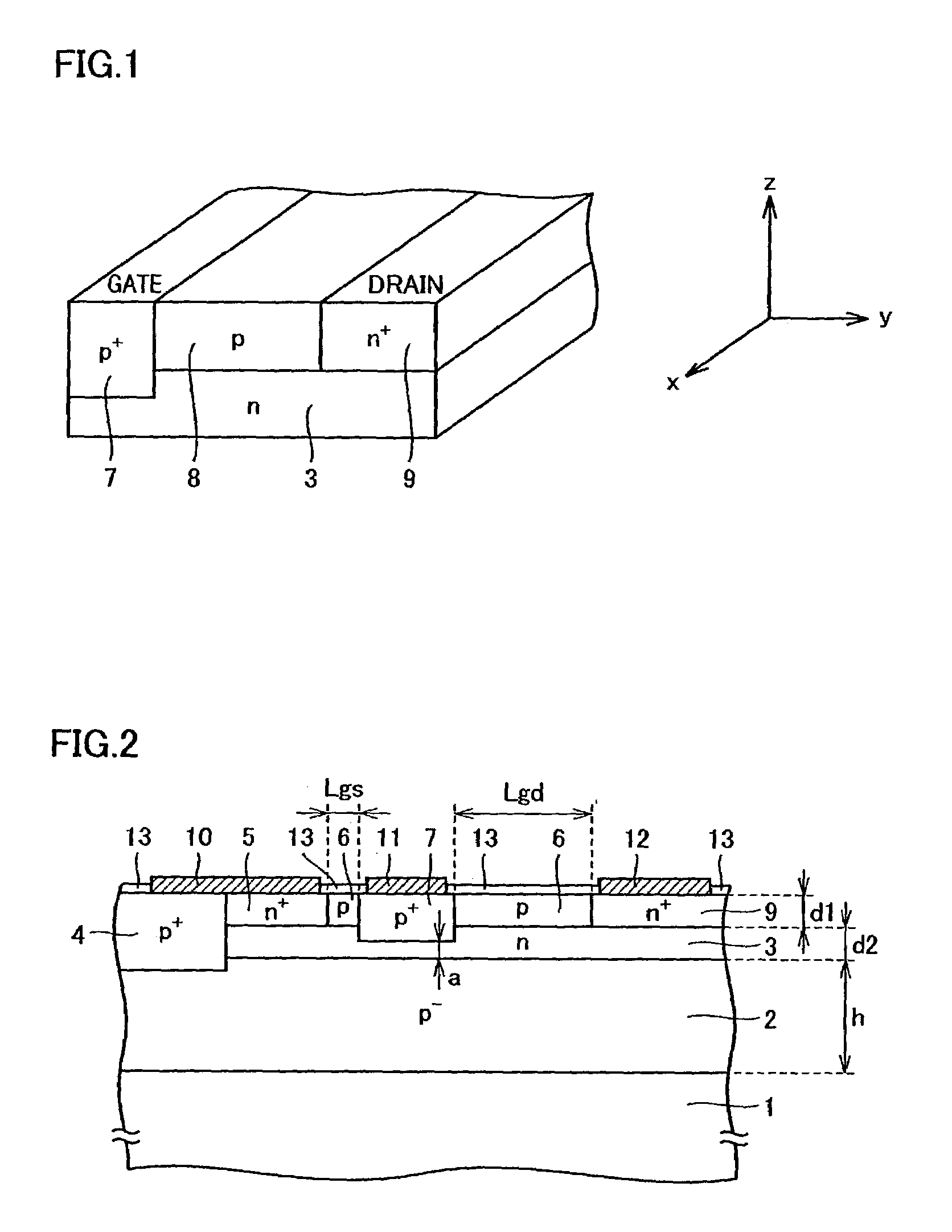
[0052]Referring to FIG. 2, a structure of a lateral JFET is described according to this embodiment. The semiconductor substrate used here is a single crystal SiC substrate of any conductivity type. On this single crystal SiC substrate 1, a p−-type epitaxial layer 2 which is a first semiconductor layer containing impurities of a first conductivity type is provided as shown in FIG. 2. On this p-type epitaxial layer 2, an n-type epitaxial layer 3 is provided that is a second semiconductor layer containing impurities of a second conductivity type with a higher concentration than that of p−-type epitaxial layer 2. On this n-type epitaxial layer 3, a p-type epitaxial layer 6 is provided that is a third semiconductor layer.

[0053]In this p-type epitaxial layer 6, an n+-type source region layer 5 and an n+-type drain region layer 9 are provided at a predetermined distance therebetween that contain impurities of the second conductivity type with a higher concentration than the impurity c...

second embodiment

[0058

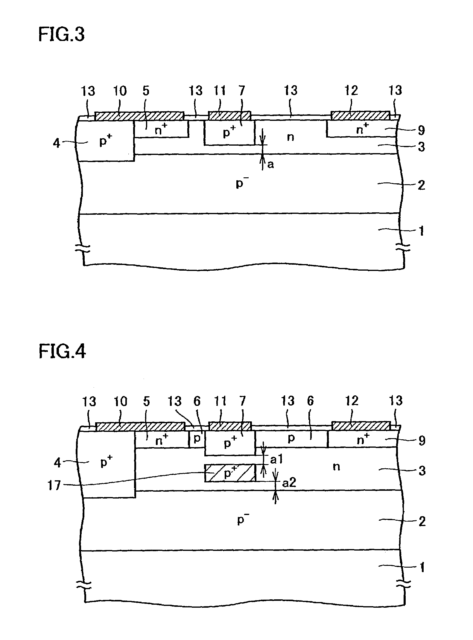
[0059]Referring to FIG. 3, a structure of a lateral JFET according to this embodiment is now described. The above-discussed lateral JFET of the first embodiment has p-type epitaxial layer 6 provided on n-type epitaxial layer 3 and n+-type source region layer 5, n+-type drain region layer 9 and p+-type gate region layer 7 are provided in this p-type epitaxial layer 6. According to the second embodiment, the lateral JFET does not include p-type epitaxial layer 6 on n-type-epitaxial layer 3 and has its n+-type source region layer 5, n+-type drain region layer 9 and p+-type gate region layer 7 formed in n-type epitaxial layer 3. This structure is the same as that of the first embodiment except for the above-described details.

[0060]The structure as described above also provides an electric field distribution which is a constant electric field similar to that of parallel-plate capacitors, instead of the electric field distribution of the normal pn junction. Accordingly, a decreased O...

third embodiment

[0062

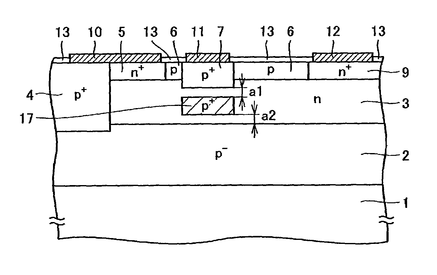
[0063]Referring to FIG. 4, a structure of a lateral JFET according to this embodiment is described. The lateral JFET of this embodiment has the same basic structure as that of the first embodiment, and one feature of the third embodiment is that one impurity injection region 17 is provided, in n-type epitaxial layer 3, between p−-type epitaxial layer 2 and p+-type gate region layer 7, and this region 17 has almost the same impurity concentration and the same potential as those of p+-type gate region layer 7.

[0064]This structure also provides an electric field distribution which is a constant electric field similar to that of parallel-plate capacitors, instead of the electric field distribution of the normal pn junction. Accordingly, a decreased ON resistance is achieved while the withstand voltage is maintained, as compared with the lateral JFET of the conventional structure.

[0065]Further, distance (a1) in this structure between the top of impurity injection region 17 and the b...


PUM


Abstract

A lateral JFET has a basic structure including an n-type semiconductor layer (3) formed of an n-type impurity region and a p-type semiconductor layer formed of a p-type impurity region on the n-type semiconductor layer (3). Moreover, in the p-type semiconductor layer, there are provided a p+-type gate region layer (7) extending into the n-type semiconductor layer (3) and containing p-type impurities of an impurity concentration higher than that of the n-type semiconductor layer (3) and an n+-type drain region layer (9) spaced from the p+-type gate region layer (7) by a predetermined distance and containing n-type impurities of an impurity concentration higher than that of the n-type semiconductor layer (3). With this structure, the lateral JFET can be provided that has an ON resistance further decreased while maintaining a high breakdown voltage performance.

Description

TECHNICAL FIELD[0001]The present invention relates to lateral junction field-effect transistors, and particularly to a lateral junction field-effect transistor having an ON resistance which can be decreased while maintaining a satisfactory breakdown voltage performance.BACKGROUND ART[0002]A junction field-effect transistor (hereinafter referred to as JFET) has a pn junction provided on either side of a channel region where carriers are passed therethrough, and a reverse bias voltage is applied from a gate electrode to extend a depletion layer from the pn junction into the channel region to control the conductance of the channel region and carry out such an operation as switching. In particular, a lateral JFET refers to the one having a channel region through which carriers move in parallel with the surface of the device.[0003]The carriers in the channel may be electrons (n-type) or holes (p-type). A JFET having a semiconductor substrate of SiC usually has a channel region which is a...

Claims


Application Information

Patent Timeline
Patent Type & Authority Patents(United States)
IPC IPC(8): H01L29/808H01L21/337H01L29/06H01L29/10H01L29/24H01L29/772
CPCH01L29/0623H01L29/808H01L29/1066H01L29/1608
Inventor HARADA, SHINHIROTSU, KENICHIMATSUNAMI, HIROYUKIKIMOTO, TSUNENOBU
Owner SUMITOMO ELECTRIC IND LTD
Why Eureka
Try Eureka