Semiconductor integrated circuit device

a technology of integrated circuits and semiconductors, applied in the direction of logic circuit coupling/interface arrangements, instruments, pulse techniques, etc., can solve the problems of extremely restricted and achieve the effect of increasing cell height, reducing the effect of negligible effect on the entire layout, and reducing the degree of freedom of signal lines

Inactive Publication Date: 2006-04-04
RENESAS ELECTRONICS CORP
View PDF4 Cites 26 Cited by
  • Summary
  • Abstract
  • Description
  • Claims
  • Application Information

AI Technical Summary

Benefits of technology

[0011]As described above, no consideration has been given to the layout for retaining data in flip-flop cells that are distributed and placed as described above also during power shutdown and for suppressing the overhead of the circuit area under the existent design environment for layout.
[0012]In accordance with the present invention, notice has been taken of the fact on that the data retention circuit for retaining data during power shutdown requires no such large current supply performance as required for normal operation, and it has been determined to supply an operation voltage by a power line that is smaller in size than the usual main power line. Preferably, the power line for the data retention circuit is considered as a signal line and is wired upon placing and routing by using CAD. This is adaptable for the CAD-assisted design environment for a layout. In this case, the power terminals for the data retention circuit are previously disposed to the cell in the same manner as for the usual signal line terminals. This no longer requires an additional layout for the power lines in the cell to enable area saving and, in addition, design by existent placing and routing tools is enabled.
[0013]The returning time from the power shutdown can be shortened drastically, and, therefor, the overhead to the circuit area can be decreased.

Problems solved by technology

On the other hand, if it is intended to further layout the main power line while fixing the height of the cell as it is by utilizing the wiring channel for signal lines, there may be a worry that the degree of freedom for the signal line is extremely restricted.

Method used


Image

  • Semiconductor integrated circuit device
  • Semiconductor integrated circuit device
  • Semiconductor integrated circuit device

Examples


Embodiment Construction

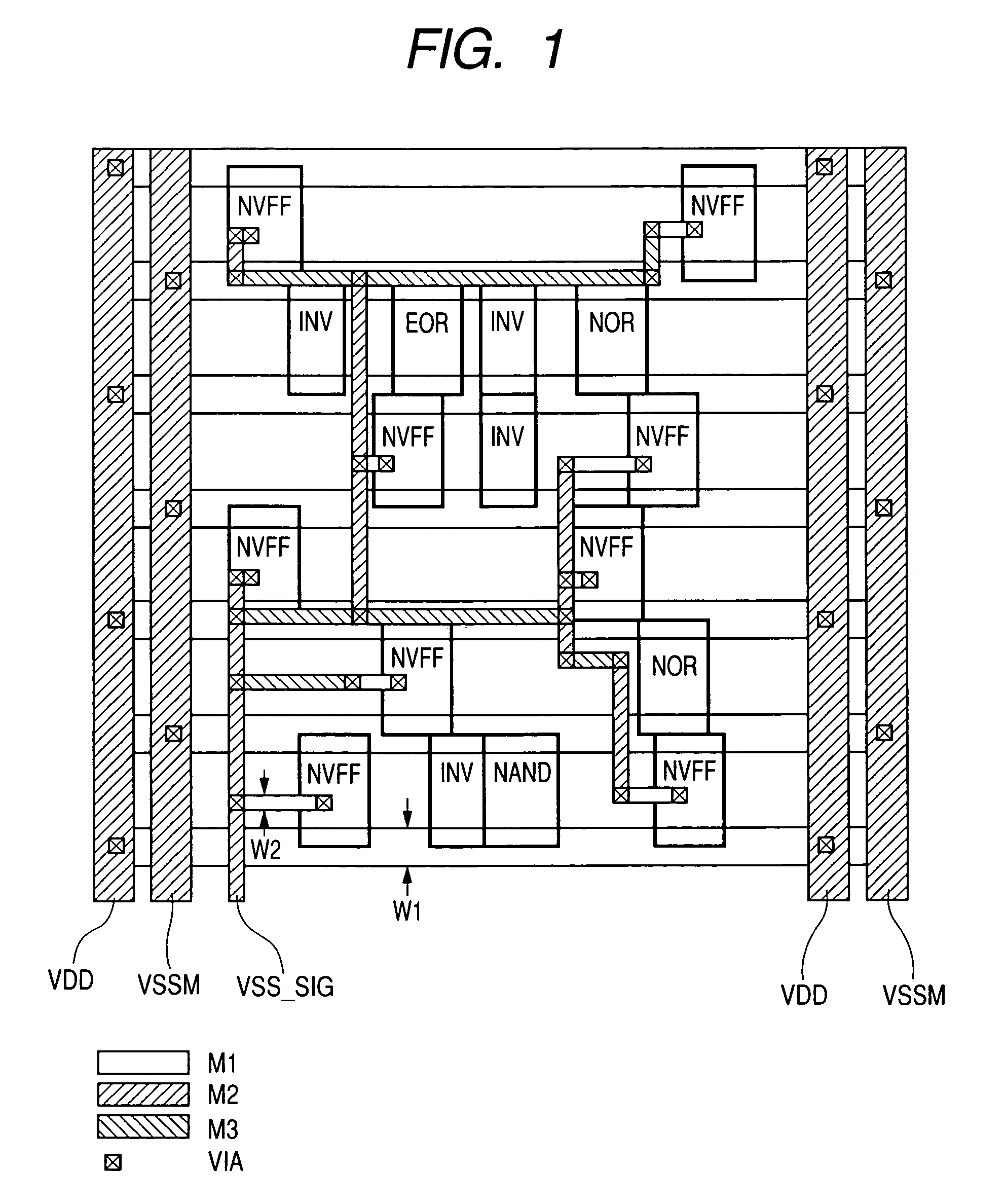
[0069]FIG. 1 shows an embodiment of a layout image of chip wirings in accordance with the present invention. The drawing shows an example in which usual main power lines, that is, power lines VDD (for example, at 1.2 V) and virtual power lines VSSM (0 V), and a power line for data retention VSS_SIG (0 V) for a nonvolatile flip-flop NVFF (hereinafter referred to nonvolatile FF) are wired. In this example, since it is assumed that the power line on the ground side (low potential side) is placed under shut down control during a standby mode, the power line on the low potential side constitutes the virtual power line VSSM. In the placing and routing tool, the virtual power line VSSM is considered as a substantial ground line of the cells. As illustrated in the drawing, the power line VSS_SIG is connected with terminals of the nonvolatile FF NVFF dispersed in a circuit block by the placing and routing tool by using CAD by way of an optional route and by using optional wiring layers.

[0070...


PUM


Abstract

In a low power consumption mode in which prior data is retained upon power shutdown, the return speed thereof is increased. While use of an existent data retaining flip-flop may be considered, this is not preferred since it increases area overhead such as enlargement of the size of a cell. A power line for data retention for power shutdown is formed with wirings finer than a usual main power line. Preferably, power lines for a data retention circuit are considered as signal lines and wired by automatic placing and mounting. For this purpose, terminals for the power line for data retention are previously designed by providing the terminals therefor for the cell in the same manner as in the existent signal lines. Additional layout for power lines is no longer necessary for the cell, which enables a decrease in the area and design by an existent placing and routing tool.

Description

CLAIM FOR PRIORITY[0001]The present application claims priority from Japanese application JP 2003-384237 filed on Nov. 13, 2003, and Japanese application JP 2004-185475 filed on Jun. 23, 2004, the contents of which are hereby incorporated by reference into this application.FIELD OF THE INVENTION[0002]The present invention concerns a semiconductor integrated circuit device which is particularly useful when applied to system LSIs or micro processors.BACKGROUND OF THE INVENTION[0003]In system LSIs used for a gizmo (personal digital assistant (PDA), hand-held device) typically represented by mobile telephones, there has been an increasing demand for long time operation by a battery of restricted capacity. Particularly, in a mobile telephone, it is extremely important to reduce the power consumption during a long waiting time (a state in which the power source is turned on, but processing under high load is not conducted) in order to satisfy the requirement for long time operation. One o...

Claims


Application Information

Patent Timeline
Patent Type & Authority Patents(United States)
IPC IPC(8): H01L29/76H01L23/48H01L21/822G11C5/06G11C11/417H01L21/82H01L27/02H01L27/04H01L27/092H01L27/118H03K3/037H03K3/356H03K3/3562H03K19/00H03K19/0175H03K19/08
CPCG01R31/318572G11C5/063G11C11/417H01L27/0207H01L27/11807H03K3/356008H03K3/35625H03K19/0016H01L27/092H01L2924/0002H01L2924/00H03K19/00H03K19/08
Inventor KANNO, YUSUKEMIZUNO, HIROYUKIIRIE, NAOHIKO
Owner RENESAS ELECTRONICS CORP
Why Eureka
Try Eureka