Trenches to reduce lateral silicide growth in integrated circuit technology

Active Publication Date: 2006-04-04
GLOBALFOUNDRIES US INC
View PDF8 Cites 6 Cited by
  • Summary
  • Abstract
  • Description
  • Claims
  • Application Information

AI Technical Summary

Benefits of technology

[0019]This method significantly lowers the electrical resistance between the contacts and the silicon or polysilicon greatly improving performance of the integrated circ

Problems solved by technology

Integrated circuits are made in and on silicon wafers by extremely complex systems that require the coordination of hundreds or even thousands of precisely controlled processes to produce a finished semiconductor wafer.
As transistors have decreased in size, it has been found that the electrical resistance between the metal contacts and the silicon substrate or the polysilicon has increased to the level where it negatively impacts the performance of the transistors.
However, existing siliciding and s

Method used


Image

  • Trenches to reduce lateral silicide growth in integrated circuit technology
  • Trenches to reduce lateral silicide growth in integrated circuit technology
  • Trenches to reduce lateral silicide growth in integrated circuit technology

Examples


Example

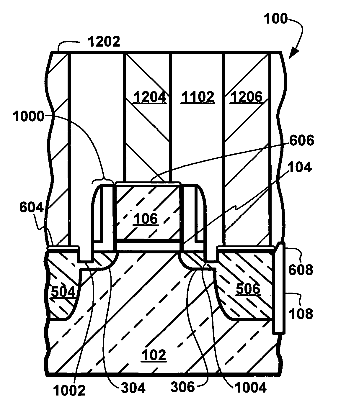
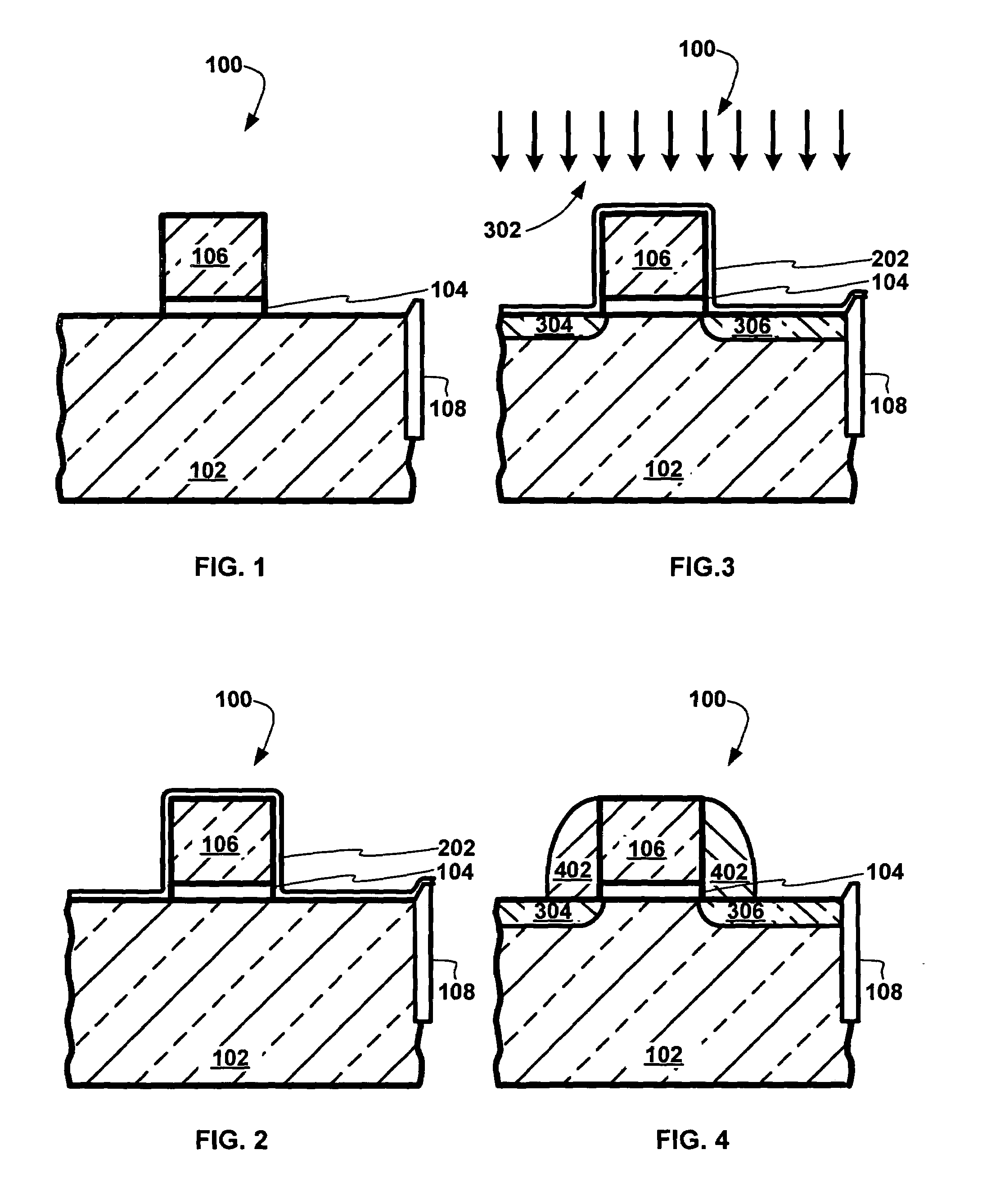
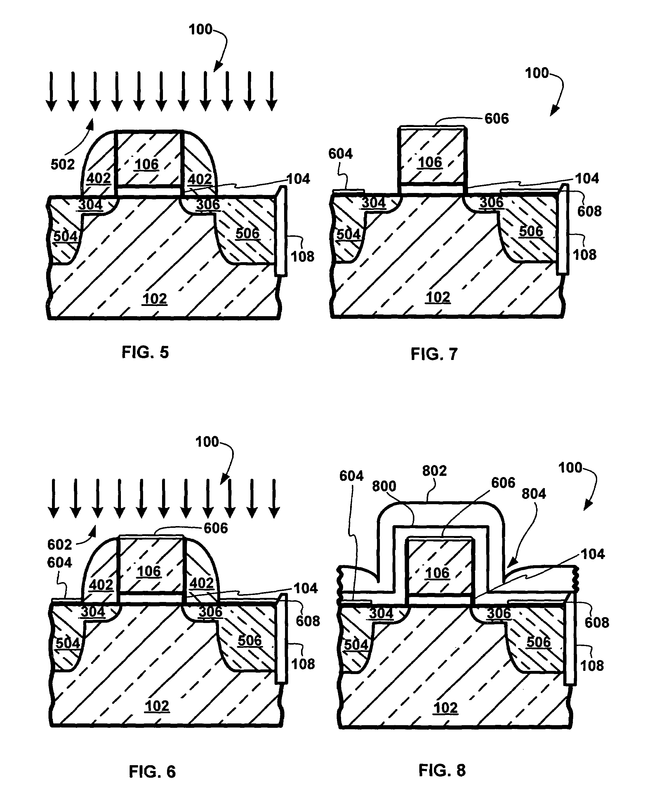
[0035]In the following description, numerous specific details are given to provide a thorough understanding of the invention. However, it will be apparent to one skilled in the art that the invention may be practiced without these specific details. In order to avoid obscuring the present invention, some well-known configurations and process steps are not disclosed in detail. In addition, the drawings showing embodiments of the apparatus are semi-diagrammatic and not to scale and, particularly, some of the dimensions are for the clarity of presentation and may be exaggerated in the drawing FIGs. The same numbers will be used in all the drawing FIGs. to relate to the same elements.

[0036]The term “horizontal” as used herein is defined as a plane parallel to a substrate or wafer. The term “vertical” refers to a direction perpendicular to the horizontal as just defined. Terms, such as “on”, “above”, “below”, “bottom”, “top”, “side” (as in “sidewall”), “higher”, “lower”, “over”, and “unde...


PUM


Abstract

A method of forming an integrated circuit with a semiconductor substrate is provided. A gate dielectric is formed on the semiconductor substrate, and a gate is formed on the gate dielectric. Source/drain junctions are formed in the semiconductor substrate. A silicide is formed on the source/drain regions and on the gate. Trenches are formed in the semiconductor substrate around the gate. An interlayer dielectric is deposited above the semiconductor substrate, and contacts are then formed to the silicide.

Description

BACKGROUND[0001]1. Technical Field[0002]The present invention relates generally to semiconductor technology, and more specifically to siliciding in semiconductor devices.[0003]2. Background Art[0004]Electronic products are used in almost every aspect of life, and the heart of these electronic products is the integrated circuit. Integrated circuits are used in everything from airplanes and televisions to wristwatches.[0005]Integrated circuits are made in and on silicon wafers by extremely complex systems that require the coordination of hundreds or even thousands of precisely controlled processes to produce a finished semiconductor wafer. Each finished semiconductor wafer has hundreds to tens of thousands of integrated circuits, each worth hundreds or thousands of dollars.[0006]Integrated circuits are made up of hundreds to millions of individual components. One common component is the semiconductor transistor. The most common and important semiconductor technology presently used is ...

Claims


Application Information

Patent Timeline
IPC IPC(8): H01L29/94
CPCH01L21/76897H01L29/66636H01L29/6653H01L29/665
Inventor CHAN, DARIN A.CHAN, SIMON SIU-SINGPATTON, JEFFREY P.BERTRAND, JACQUES J.
Owner GLOBALFOUNDRIES US INC
Why Eureka
Try Eureka