Air-gap insulator for short-term exposure to a high temperature environment

a technology of air gap insulation and high temperature environment, which is applied in the direction of casings/cabinets/drawers, casings/cabinets/drawers, instruments, etc., can solve the problems of limiting the use of electronic circuitry in many places, harming their own performance, and harsh environmental conditions, etc., to achieve the effect of maintaining operability

Inactive Publication Date: 2006-04-04
HONEYWELL INT INC
View PDF12 Cites 17 Cited by
  • Summary
  • Abstract
  • Description
  • Claims
  • Application Information

AI Technical Summary

Benefits of technology

[0010]A packaging system for electronic circuitry, which may be disposed on a substrate, is provided. The packaging system includes a combination of (i) an inner housing, which may surround the substrate, (ii) an outer housing, which may surround the inner housing and the substrate combination, (iii) and a gap positioned between the inner and outer housings. The gap may be filled with insulating media, such as air. The combination of the inner housing, the outer housing, and the gap allow the electronic circuitry to maintain operability during and after the packaging system experiences short term exposure to a high temperature.

Problems solved by technology

Many modern electronic circuits begin to exhibit problems at external temperatures between about 80 and 100 degrees C., and begin to fail at temperatures barely above 100 degrees C. Consequently, additional environmental temperature conditions acting upon the electrical components can raise the temperature of the components above their operation thresholds, which unfortunately limits using electronic circuitry in many desirable, but harsh environmental condition locations.
Excessive heat generated or applied during operation of these components can not only harm their own performance, but can also degrade the performance and reliability to the point of failure of overall systems that include such components.
The increasingly wide range of environmental conditions, including temperature extremes, in which electronic systems are expected to operate, intensifies these negative effects.
For instance, when the temperatures of the electronic components rise above the operational-threshold temperatures for even a short time, junctions of silicon devices can fail, solder pads can reflow thereby causing undesirable cold solder joints, thermistors and other temperature sensing components can shift thereby causing the electronics to become inoperable, printed circuit boards and the materials thereof can become malleable and be easily damaged, and other electromechanical failures can occur.
Limitations exist, however, with the use of heat sinks.
First, heat sinks can become large, as heat sinks seek to increase the heat transfer efficiency between the components and the ambient air by primarily increasing the surface area that is in direct contact with the air.
The size constraints of the heat sinks and other associated electronic circuitry greatly limit reduction of electronic packaging and thereby hinder placing electronic circuitry in small locations.
Second, due to inefficient heat-sink-to-air heat transfer, damage to the underlying electronic circuitry can occur before the heat sink can react.
And as the external temperature is applied to such heat sinks, the heat transfer to the circuitry may be delayed due to the thermal conductivity of the heat sink.
Thus, any potential advantages of external temperature sensors used to protect the underlying circuitry may be thwarted.

Method used


Image

  • Air-gap insulator for short-term exposure to a high temperature environment
  • Air-gap insulator for short-term exposure to a high temperature environment
  • Air-gap insulator for short-term exposure to a high temperature environment

Examples


Embodiment Construction

[0015]In the following detailed description, numerous specific details are set forth in order to provide a thorough understanding of the invention. However, it will be understood that the present invention may be practiced without these specific details. In other instances, well-known methods, procedures, components and circuits have not been described in detail, so as not to obscure the present invention. Further, the presently preferred embodiments disclosed are for exemplary purposes only and other embodiments may be employed in lieu of or in combination with the embodiments disclosed.

[0016]1. Exemplary Architecture

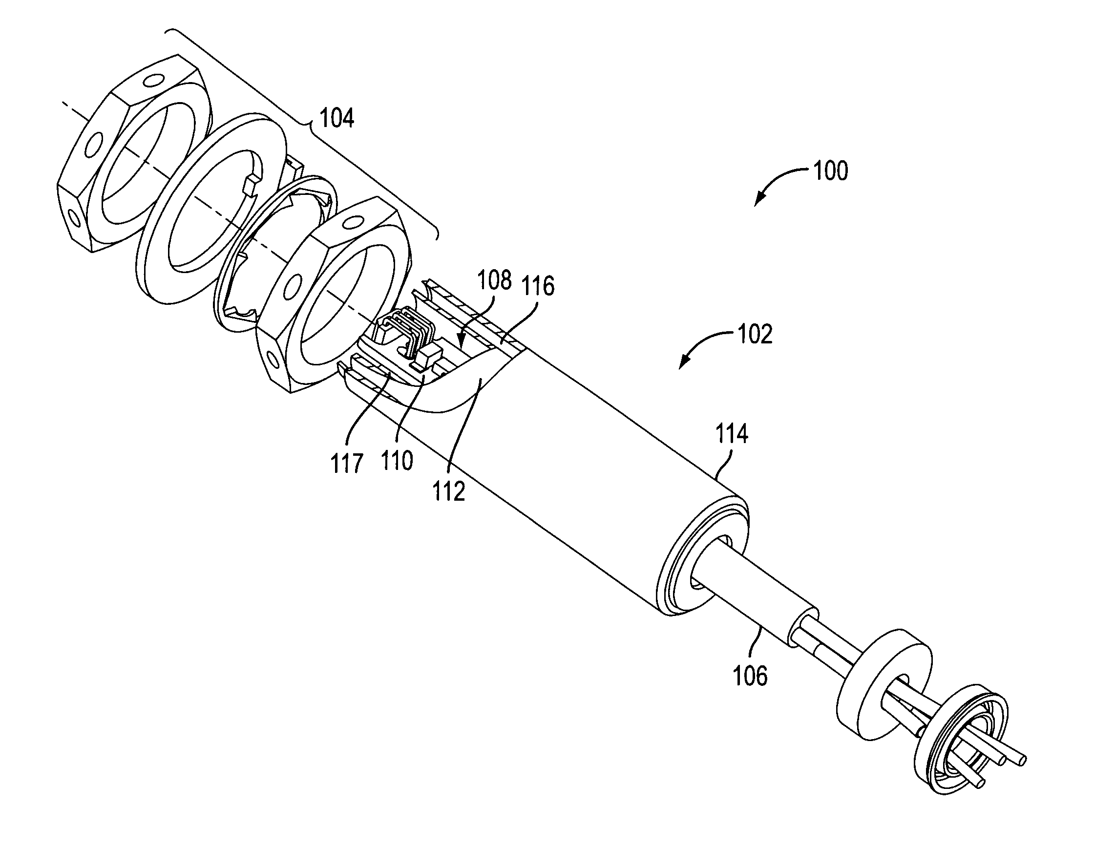
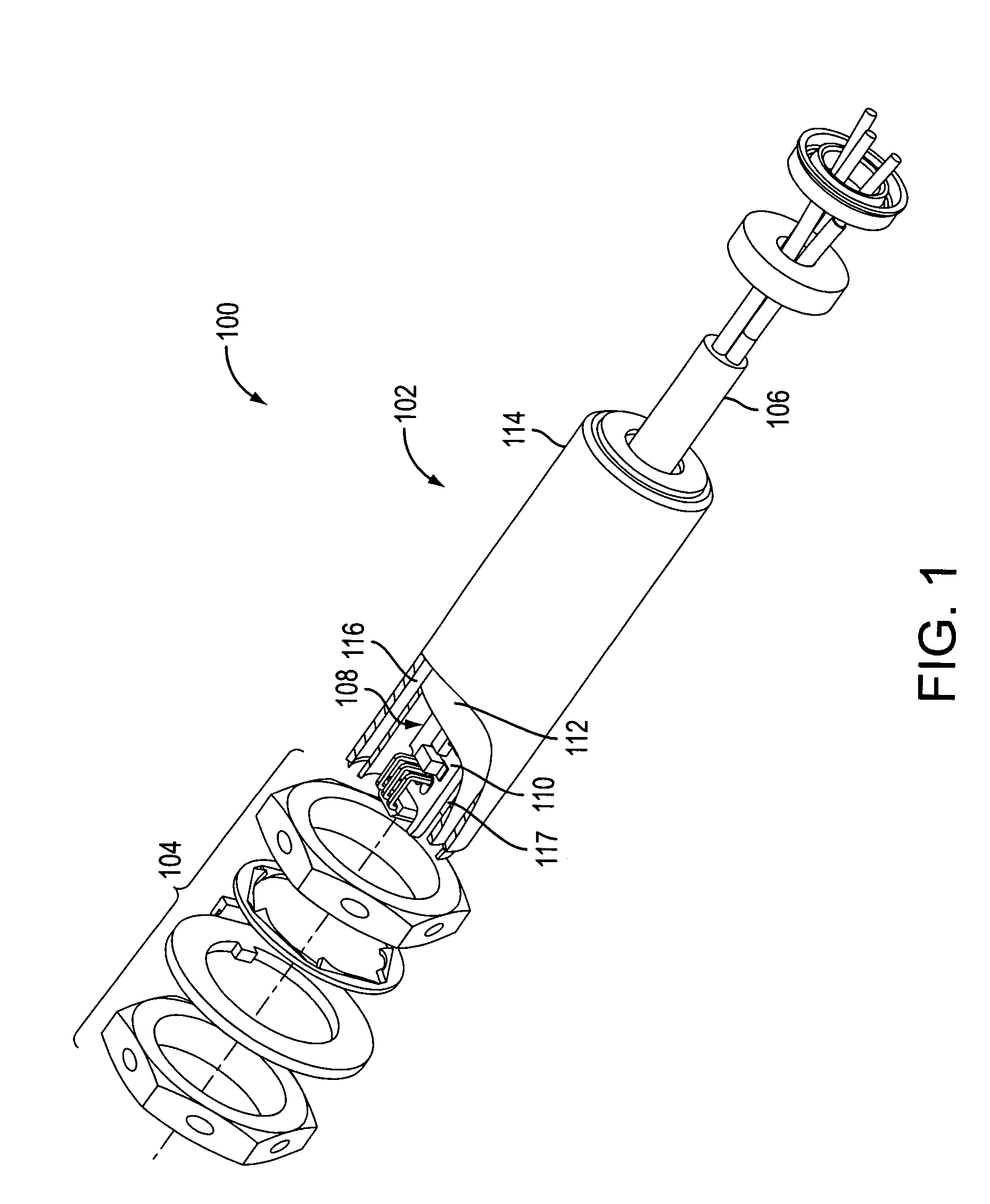
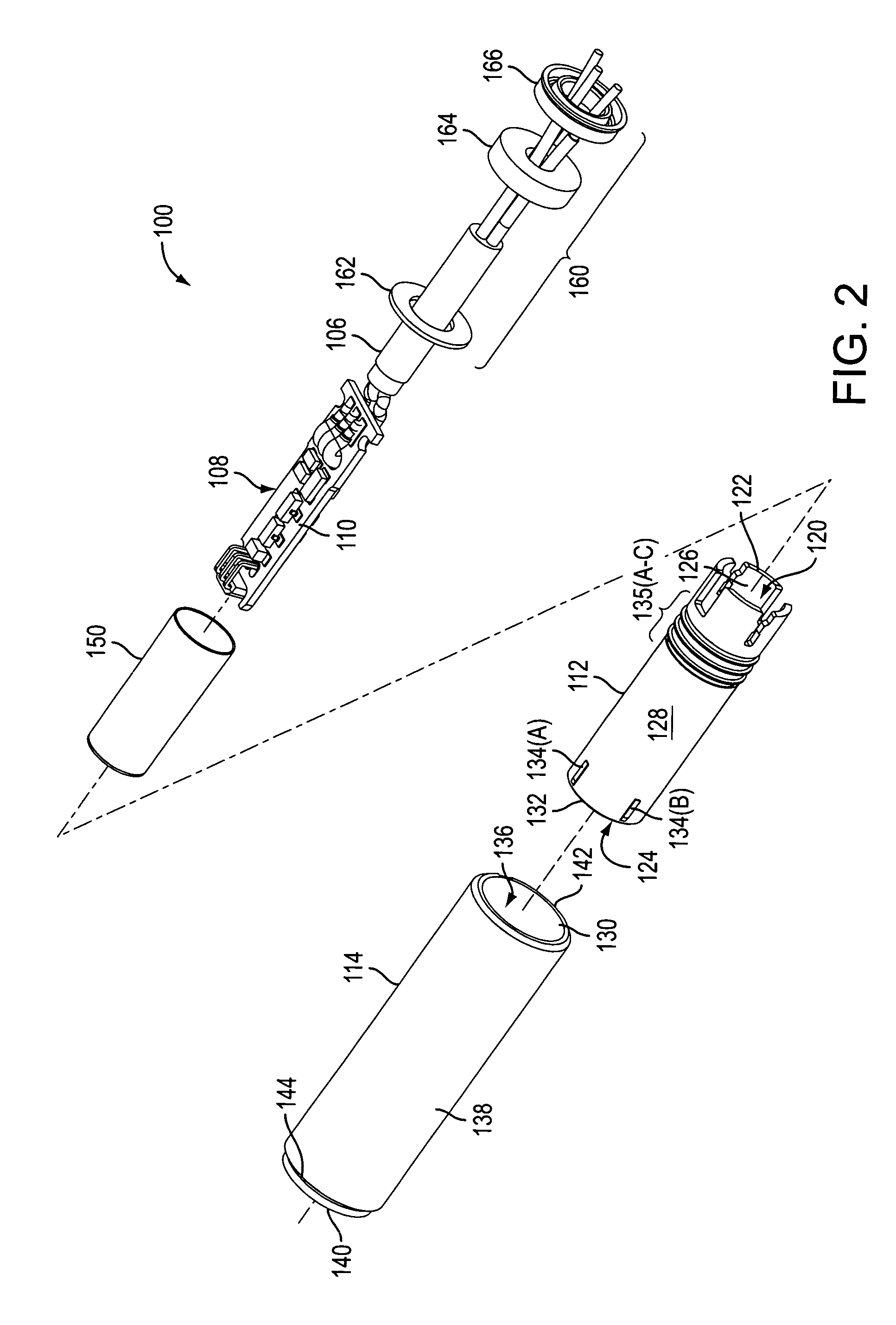
[0017]FIG. 1 illustrates an isometric view of an electronic module 100 incorporating a packaging system in accordance with an exemplary embodiment. The exemplary electronic module 100 shown in FIG. 1 includes a packaging system 102 and mounting hardware 104 for mounting the packaging system 102 to an external device, such as an aircraft. The electronic module 100 also ...


PUM


Abstract

A packaging system for electronic circuitry is provided. The electronic circuitry may be disposed upon a substrate, which can be encased or otherwise surrounded by one or more components of the packaging system. The packaging system may include (i) an inner housing that can encase or otherwise enclose the substrate within its confines; (ii) an outer housing that in turn encases or encloses the combination of the inner housing and the substrate within its confines; and (iii) one or more gaps positioned between the electronic circuitry, inner housing and outer housing. The gaps may be filled with fluid or solid insulating media. The combination of the inner housing, outer housing, and gaps can insulate the electronic circuitry from the detrimental and destructive heating effects when the packaging system experiences short-term exposure to a high temperature, which thereby allows operability before, during and after such exposure.

Description

FIELD[0001]The present invention relates generally to packaging of electronic circuitry, and more particularly, to packaging of electronic circuitry that allows the electronic circuitry to continue operation after exposure to high temperatures for a short period of time. The invention is especially useful in commercial and / or military aviation applications in which high-temperature environmental conditions can exist for short periods of time during aircraft use, such as take-off and landing.BACKGROUND[0002]With the development of sophisticated electronic components, including those capable of increasing processing speeds and higher frequencies, having smaller size and more complicated power requirements, relatively high internal temperatures can be generated within the electronic components themselves. These high internal temperatures may become more exacerbated as microprocessors, integrated circuits, and other small feature electrical components and systems are integrated into or ...

Claims


Application Information

Patent Timeline
Patent Type & Authority Patents(United States)
IPC IPC(8): G06F1/16G01D11/24H05K5/02H05K7/14
CPCH05K7/1434H05K5/0213H05K5/0209
Inventor MCCOLLUM, DAVE R.EHLERS, WAYNE L.SKARLUPKA, MICHAEL J.
Owner HONEYWELL INT INC
Why Eureka
Try Eureka