Mixed-mode optical proximity correction

a technology of optical proximity correction and mixed-mode optical proximity, which is applied in the direction of photomechanical treatment originals, instruments, photomechanical equipment, etc., can solve the problems of line-end pullback, significant design challenges, and manufacturing challenges, and achieve the effect of reducing the cost of manufacturing

Inactive Publication Date: 2006-04-04
COBB NICOLAS B
View PDF79 Cites 76 Cited by
  • Summary
  • Abstract
  • Description
  • Claims
  • Application Information

AI Technical Summary

Problems solved by technology

Reliably manufacturing these highly integrated ICs, however, presents significant design challenges.
Manufacturing challenges tend to arise when critical dimensions (the minimum distance between edges of various types of features in various regions in the IC design) approach, or drop below, the wavelength of the light source used to expose the resist.
Typical problems include line-end pullback and line-width variations that depend on the local pattern density and topology.
In many places, not enough light passed through the mask to adequately expose the resist, causing the features to overlap.
Proximity distortions, such as those illustrated in FIG. 1B, can reduce operating speed, or prevent operation entirely, due to breaks in connectivity and short circuits.
As IC designs become more complex, manual OPC (entering corrections by hand through trial and error) becomes more time consuming and less cost effective.
Model-based OPC can be very computationally intensive.
Line width variations, such as the variation over the length of feature 310B, can cause significant problems.

Method used


Image

  • Mixed-mode optical proximity correction
  • Mixed-mode optical proximity correction
  • Mixed-mode optical proximity correction

Examples


Embodiment Construction

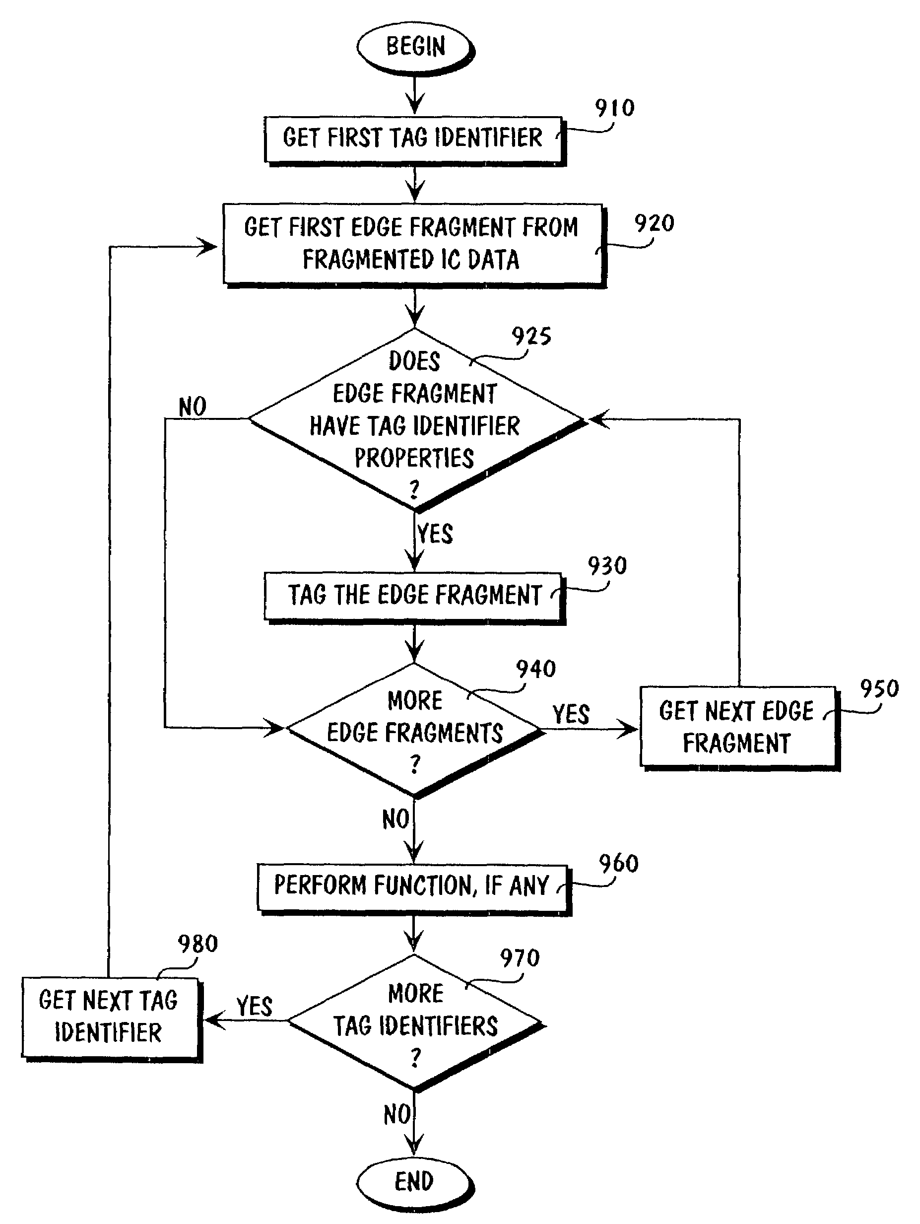
[0037]In the following detailed description, numerous specific details are set forth in order to provide a thorough understanding of the present invention. However, those skilled in the art will understand that the present invention may be practiced without these specific details, that the present invention is not limited to the depicted embodiments, and that the present invention may be practiced in a variety of alternate embodiments. In other instances, well known methods, procedures, components, and circuits have not been described in detail.

[0038]Parts of the description will be presented using terminology commonly employed by those skilled in the art to convey the substance of their work to others skilled in the art. Also, parts of the description will be presented in terms of operations performed through the execution of programming instructions. As well understood by those skilled in the art, these operations often take the form of electrical, magnetic, or optical signals cap...


PUM

PropertyMeasurementUnit
path widthaaaaaaaaaa
distanceaaaaaaaaaa

Abstract

A mask is prepared by processing design data with various combinations of rule-based and model-based optical proximity correction. In one embodiment, the design data is first processed with a set of optical proximity correction rules to produce a rule-corrected design. The rule-corrected design is examined to identify a set of features to process with model-based optical proximity correction. Then, the set of features are processed with the model-based optical proximity correction.

Description

[0001]This is a divisional of U.S. application Ser. No. 09 / 302,700, filed Apr. 30, 1999 now U.S. Pat. No. 6,467,076.FIELD OF THE INVENTION[0002]The present invention pertains to the field of integrated circuit (IC) design. More particularly, this invention relates to the art of designing deep submicron ICs.BACKGROUND OF THE INVENTION[0003]Since the advent of the integrated circuit (IC), circuit components have become smaller and smaller. An IC may include millions of components packed into an incredibly small package. With each new generation of smaller integration, more functionality, and therefore more value, can be derived from ICs. Reliably manufacturing these highly integrated ICs, however, presents significant design challenges.[0004]Those skilled in the art will be familiar with numerous processes for manufacturing ICs. For example, most ICs begin with a silicon wafer, and transistors are built one layer at a time in the silicon through repeated applications of photo exposure...

Claims


Application Information

Patent Timeline
Patent Type & Authority Patents(United States)
IPC IPC(8): G06F17/50G03F1/00G03F1/36G03F7/20
CPCG03F1/144G03F7/70541G03F7/70441G03F1/36
Inventor COBB, NICOLAS B.
Owner COBB NICOLAS B
Why Eureka
Try Eureka