Liquid manufacturing processes for panel layer fabrication
What is Al technical title?
Al technical title is built by PatSnap Al team. It summarizes the technical point description of the patent document.
a technology of panel layer and fabrication process, which is applied in the manufacture of electric discharge tubes/lamps, instruments, television systems, etc., can solve the problems of gas leakage, type of open display structure, and high end product cos
Inactive Publication Date: 2006-04-11
LEIDOS
View PDF159 Cites 46 Cited by
Summary
Abstract
Description
Claims
Application Information
AI Technical Summary
This helps you quickly interpret patents by identifying the three key elements:
Problems solved by technology
Method used
Benefits of technology
[0009]According to the present invention, a novel flexible plasma display panel and methods for making such a panel involve a web fabrication process. In this display panel, the plasma forming gas is sealed in transparent micro-components formed of a closed transparent shell. The micro-components, which may be spheres, capillaries or virtually any other three-dimensional shape, are then coated with phosphors to emit one of the primary colors: red, green or blue. In the web fabrication process, a non-conductive flexible first substrate has electrodes imprinted thereon using known printing techniques, such as lithography or screen printing. In one variation, dimples are embossed in the first substrate to define locations at which micro-components are to be placed relative to the electrodes. In another variation, the micro-components are electrostatically drawn to the correct locations relative to the electrodes. After affixing the micro-components in place, and possibly testing to ensure complete and proper placement of the micro-components, a second substrate, also in web form, is disposed over the first substrate so that the micro-components are sandwiched between the first and second substrates. Additional electrodes may be patterned on the second substrate, and the second substrate may be applied as more than one layer to create one or more dielectric / electrode sandwiches near the micro-component to provide additional sustain electrodes or addressing electrodes. Alternatively, the second substrate can be preformed with embedded electrodes which are then aligned with the micro-components when the second substrate is applied. A protective layer may be placed on top of the second substrate, then the layered assembly is diced to form individual light-emitting panels of the desired size.
Problems solved by technology
Although widely used, this type of open display structure suffers from numerous disadvantages.
The sealing of the outer edges of the parallel plates and the introduction of the plasma forming gas are both expensive and time-consuming processes, resulting in a costly end product.
In addition, it is particularly difficult to achieve a good seal at the sites where the electrodes are fed through the ends of the parallel plates, which can result in gas leakage and a shortened product life.
Another disadvantage is that individual pixels are not segregated within the parallel plates.
As a result, gas ionization activity in a selected pixel during a write operation may spill over to adjacent pixels, thereby raising the undesirable prospect of possibly igniting adjacent pixels.
In addition, in this type of display panel it is difficult to properly align the electrodes and the gas chambers, which may cause pixels to misfire.
As with the open display structure, it is also difficult to get a good seal at the plate edges.
Furthermore, it is expensive and time consuming to introduce the plasma producing gas and seal the outer edges of the parallel plates.
Method used
Image
Click on the blue label to locate the original text in one second.
Reading with bidirectional positioning of images and text.
Examples
Embodiment Construction
[0031]As embodied and broadly described herein, the preferred embodiments of the present invention are directed to a novel method for making a light-emitting panel. In particular, preferred embodiments are directed to web fabrication processes for manufacturing light-emitting panels.
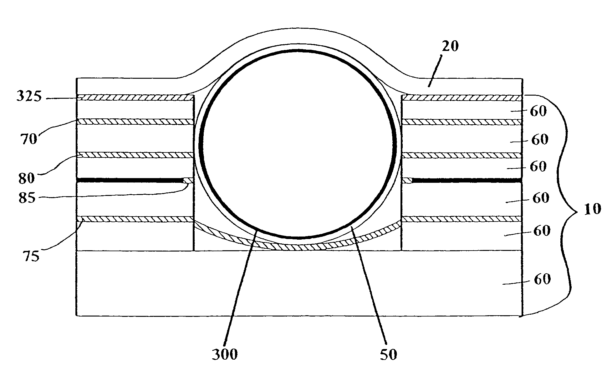
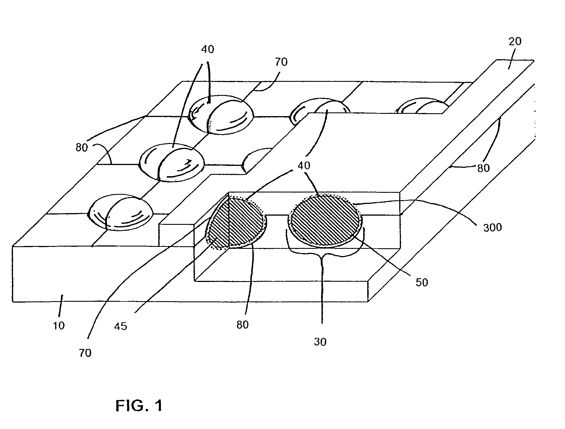
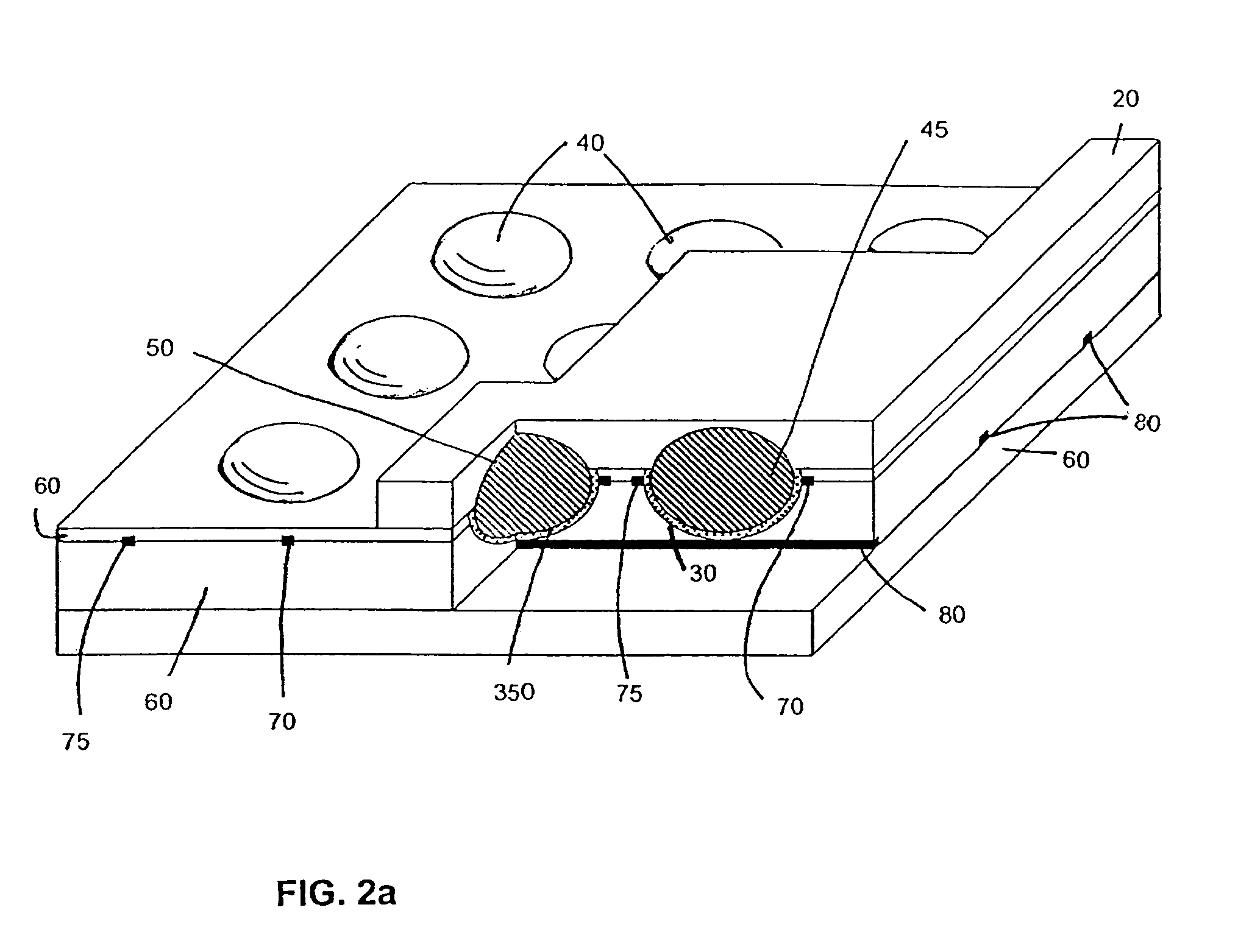
[0032]FIG. 1 illustrates an exemplary display panel in which a plurality of sphere-shaped micro-components 40 are embedded within a sandwich of dielectric layers consisting of first substrate 10 and second substrate 20. The first substrate 10 is formed from a flexible sheet material that is appropriate for web fabrication, such as polyester (e.g., Mylar®), polyimide (e.g., Kapton®), polypropylene, polyethylene, propylene, nylon or any polymer-based material possessing dielectric properties appropriate for use as an insulator between electrodes as needed for operation of a plasma display panel. Such electrical requirements are known to those of skill in the art. Second substrate 20 may be made from the sa...
PUM
Property
Measurement
Unit
radiating wavelengths
aaaaa
aaaaa
radiating wavelengths
aaaaa
aaaaa
diameter
aaaaa
aaaaa
Abstract
A method for manufacturing a light-emitting panel sandwiches a plurality of micro-components between two flexible substrates in a web configuration. Each micro-component contains a gas or gas-mixture capable of ionization when a sufficiently large voltage is supplied across the micro-component via at least two electrodes. The micro-components are disposed in sockets formed at pre-determined locations in a first dielectric substrate so that they are adjacent to electrodes imprinted in the first substrate. Dielectric layers and the conductors for acting as electrodes are formed using liquid processes or combined liquid and sheet processes, where liquid materials are applied to the surface of the underlying layer, then cured to complete the formation of layers. The assembled layers are coated with a protective coating and may include an RF shield. In one embodiment, patterning of the conductors is achieved by applying conductive ink using an ink jet process. In another embodiment, the conductors may be patterned photolithographically using a leaky optical waveguide as a contact mask.
Description
CROSS-REFERENCE TO RELATED APPLICATIONS[0001]This application is a continuation of application Ser. No. 10 / 214,740, filed Aug. 9, 2002, now U.S. Pat. No. 6,764,367 entitled Liquid Manufacturing Processes for Panel Layer Fabrication, which is a continuation-in-part of application Ser. No. 09 / 697,344, filed Oct. 27, 2000, now U.S. Pat. No. 6,612,889, entitled Method for Making a Light-Emitting Panel, and is related to the following co-owned applications: Ser. No. 09 / 697,346, now U.S. Pat. No. 6,545,422, filed Oct. 27, 2000, entitled A Socket for Use with a Micro-Component in a Light-Emitting Panel; Ser. No. 09 / 697,358, filed Oct. 27, 2000, entitled: A Micro-Component for Use in a Light-Emitting Panel; Ser. No. 09 / 697,498, filed Oct. 27, 2000, now U.S. Pat. No. 6,620,012, entitled A Method for Testing a Light-Emitting Panel and the Components Therein; Ser. No. 09 / 697,345, filed Oct. 27, 2000, now U.S. Pat. No. 6,570,335, entitled A Method and System for Energizing a Micro-Component In ...
Claims
Application Information
Patent Timeline
Application Date:The date an application was filed.
Publication Date:The date a patent or application was officially published.
First Publication Date:The earliest publication date of a patent with the same application number.
Issue Date:Publication date of the patent grant document.
PCT Entry Date:The Entry date of PCT National Phase.
Estimated Expiry Date:The statutory expiry date of a patent right according to the Patent Law, and it is the longest term of protection that the patent right can achieve without the termination of the patent right due to other reasons(Term extension factor has been taken into account ).
Invalid Date:Actual expiry date is based on effective date or publication date of legal transaction data of invalid patent.