Pattern forming method and method for manufacturing semiconductor device

a technology of semiconductor devices and forming methods, which is applied in the field of pattern transfer processes, can solve the problems of short wavelength, difficult to develop resist films having a high light transmittance for such a very short wavelength, and decrease the resistance of resist films to dry etching

Inactive Publication Date: 2006-04-11
KK TOSHIBA
View PDF21 Cites 11 Cited by
  • Summary
  • Abstract
  • Description
  • Claims
  • Application Information

AI Technical Summary

Benefits of technology

[0017]FIG. 3 is a graph simplifying the graph of FIG. 2 by binarization;

Problems solved by technology

The F2 laser, however, has a very short wavelength, and it is very difficult to develop a resist film having a high light transmittance for such a very short wavelength.
If the resist film is thinned, however, the resistance of the resist film to dry etching decreases, and it becomes difficult to achieve high performance both in the resistance to dry etching and the resolution.
Further, in a resist pattern forming method using a low-acceleration electron beam instead of a laser, the distance of transmission of an electron beam in the resist film is short.
It is thus difficult to increase the thickness of the resist film.
The above-described method using the buried material, however, has the following problem.
This would pose a problem in controlling processing dimensions when an underlying film 103 is processed.
In this case, however, it is difficult to control the in-plane uniformity in etch-back depth.
This may lead to failure in the application of ordinary etching techniques.

Method used


Image

  • Pattern forming method and method for manufacturing semiconductor device
  • Pattern forming method and method for manufacturing semiconductor device
  • Pattern forming method and method for manufacturing semiconductor device

Examples


first embodiment

(First Embodiment)

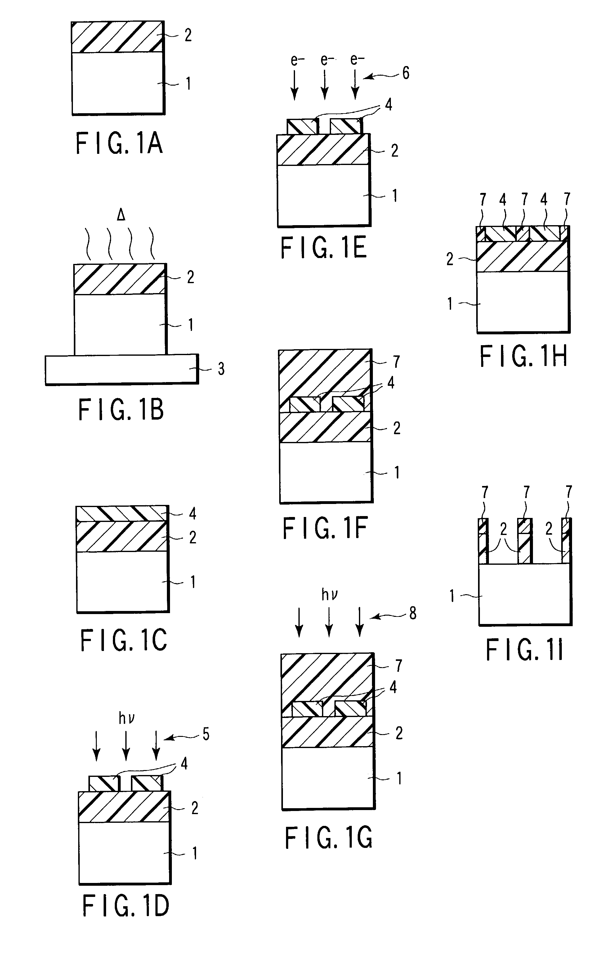
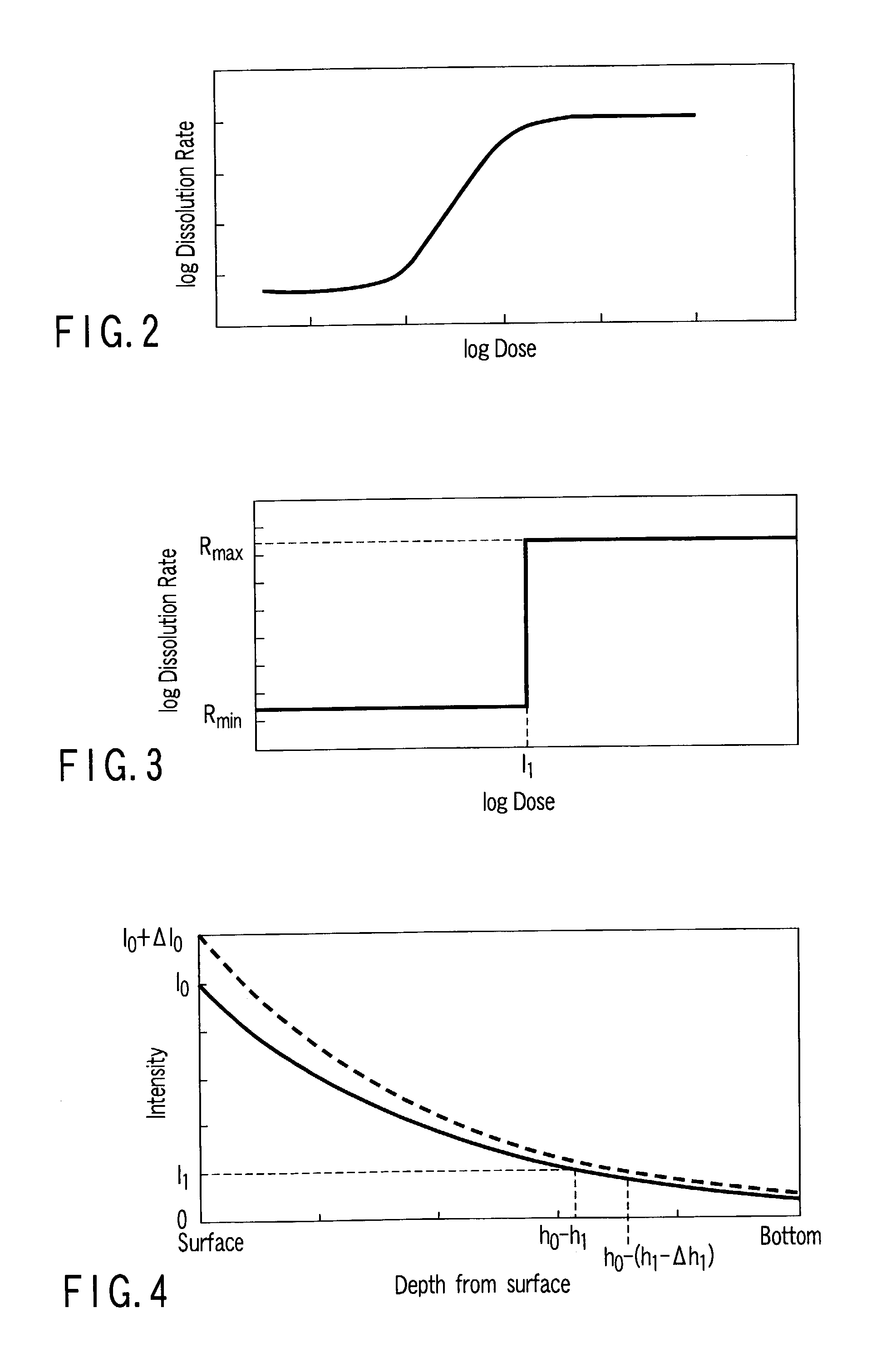
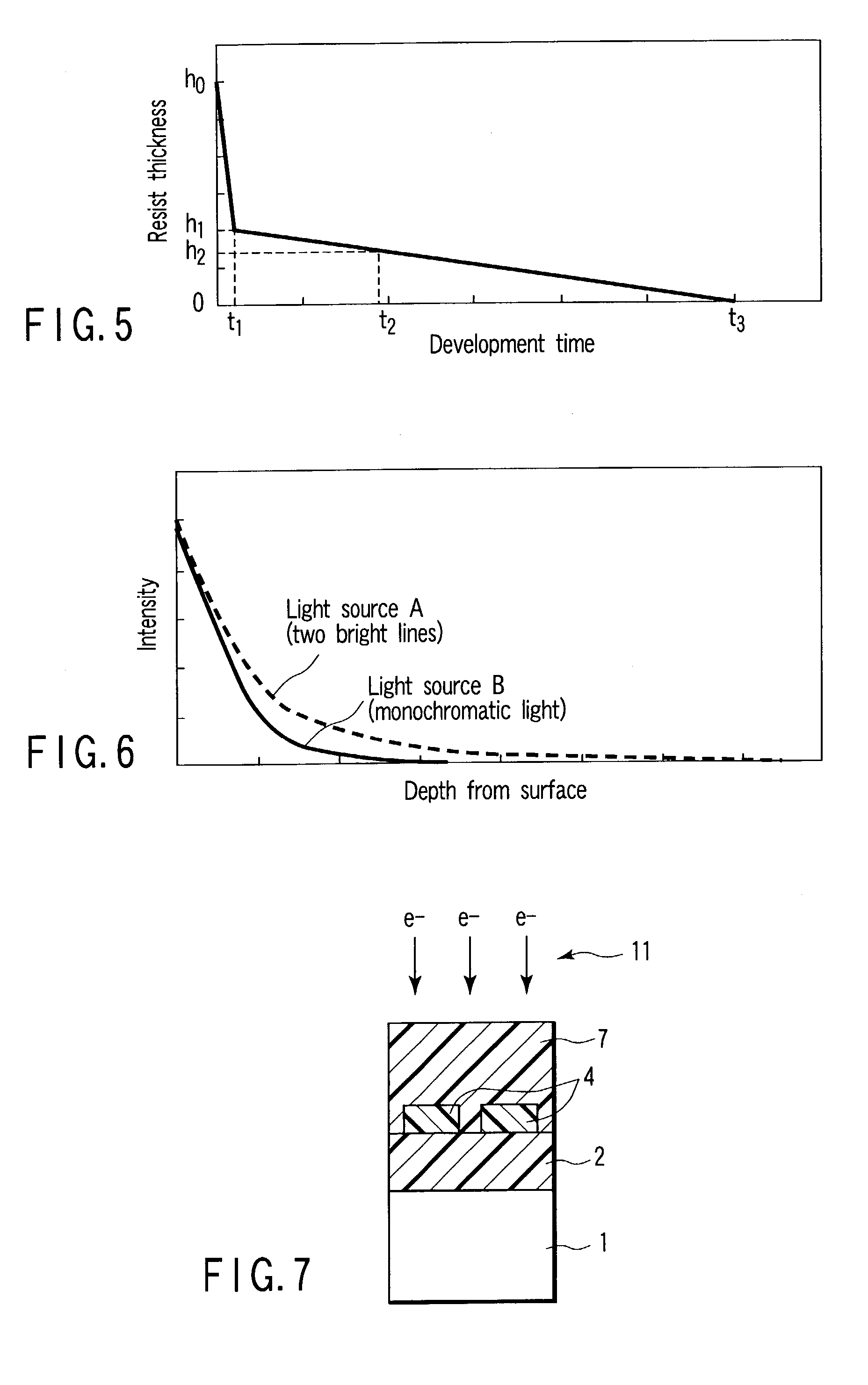
[0034]A first embodiment of the present invention will be described with reference to FIGS. 1A to 1I and FIGS. 2 to 6. FIG. 1A to FIG. 1I are cross-sectional views illustrating steps of a pattern forming method according to the first embodiment. FIG. 2 is a graph showing the relationship between a resist dissolution rate and an exposure amount (dose). FIG. 3 is a graph simplifying the graph of FIG. 2 by binarization. FIG. 4 is a graph showing a light intensity distribution in a depth direction in a case where a buried material is exposed with monochromatic light. FIG. 5 is a graph showing the relationship between a development time of a buried material and a residual film thickness (resist thickness). FIG. 6 is a graph showing a light intensity distribution in a depth direction in a case where a resist film is exposed with light components of plural wavelengths.

[0035]In the first embodiment, An ArF positive resist film is used as a resist film. A photosensitive pol...

second embodiment

(Second Embodiment)

[0080]A second embodiment of the present invention will now be described with reference to FIG. 7. FIG. 7 is a cross-sectional view depicting a step in a pattern forming method according to the second embodiment. The parts common to those in FIGS. 1A to 1I are denoted by like reference numerals, and a detailed description thereof is omitted. A semiconductor device manufacturing method according to the second embodiment is the same as the above-described semiconductor device manufacturing method according to the first embodiment, so a description thereof is omitted. The same applies to the descriptions of third to eighth embodiments which will follow.

[0081]The ArF excimer laser beam 8 with a wavelength of about 193 nm is used in the first embodiment in the all-surface exposure step of applying a radiation to the photosensitive polysilazane used as the positive-type radiosensitive compound film. In the second embodiment, the ArF excimer laser beam 8 is replaced with...

third embodiment

(Third Embodiment)

[0084]A third embodiment of the present invention will now be described with reference to FIGS. 8A to 8H. FIGS. 8A to 8H are cross-sectional views showing steps of a pattern forming method according to the third embodiment.

[0085]In the third embodiment, a DLC (Diamond Like Carbon) film is used as a to-be-processed film. A negative resist film for low-acceleration EB write is used as a resist film. Poly [p-(1,2-dimethyl diphenyl disilanylene)phenylene] is used as the buried material. A low-pressure mercury lamp is used as a light source for irradiating the buried material. The details of the third embodiment will follow.

[0086]To start with, as shown in FIG. 8A, a DLC (Diamond Like Carbon) film 21 with a thickness of about 0.3 μm, serving as a to-be-processed film, is provided on a semiconductor substrate 1.

[0087]Next, as shown in FIG. 8B, a low-acceleration EB write negative resist film 22 serving as a resist film is spin-coated on the DLC film 21 so as to have a th...


PUM

PropertyMeasurementUnit
light absorption coefficientaaaaaaaaaa
thicknessaaaaaaaaaa
thicknessaaaaaaaaaa

Abstract

A pattern forming method is disclosed which comprises providing a to-be-processed film on a substrate, providing a resist film on the to-be-processed film, patterning the resist film, providing a film of a radiosensitive compound on the to-be-processed film such that the patterned resist film is covered with the film of the radiosensitive compound, subjecting the film of the radiosensitive compound to irradiation and a development process, thus exposing an upper surface of the resist film and patterning the film of the radiosensitive compound, and removing the resist film and processing the to-be-processed film, using the patterned film of the radiosensitive compound as a mask.

Description

CROSS-REFERENCE TO RELATED APPLICATIONS[0001]This application is based upon and claims the benefit of priority from the prior Japanese Patent Application No. 2002-122862, filed Apr. 24, 2002, the entire contents of which are incorporated herein by reference.BACKGROUND OF THE INVENTION[0002]1. Field of the Invention[0003]The present invention relates generally to a pattern transfer process, and more particularly to a pattern forming method with improved processing precision for a to-be-processed film on which a pattern is to be transferred, and a method of manufacturing a semiconductor device using a pattern formed by this pattern forming method.[0004]2. Description of the Related Art[0005]In general, in a lithography step in a series of steps of a semiconductor device manufacturing process, a resist pattern is used as a mask for dry etching in order to process a to-be-processed film lying under the mask. The resist film is thus required to have high performance in both resolution an...

Claims


Application Information

Patent Timeline
Patent Type & Authority Patents(United States)
IPC IPC(8): G03F7/00G03F7/26G03F7/075G03F7/40H01L21/027
CPCG03F7/0035H01L21/0275H01L21/0279H01L21/0278H01L21/0277
Inventor KATO, HIROKAZUONISHI, YASUNOBUSHIOBARA, EISHIKAWAMURA, DAISUKENAKAMURA, HIROKO
Owner KK TOSHIBA
Why Eureka
Try Eureka