Dynamic random access memory cell and fabrication thereof

Inactive Publication Date: 2006-04-11
PROMOS TECH INC
View PDF1 Cites 3 Cited by
  • Summary
  • Abstract
  • Description
  • Claims
  • Application Information

AI Technical Summary

Benefits of technology

[0007]In view of the foregoing, on aspect of this invention is to provide a dynamic random access memory (DRAM) cell that has a capacitor for

Problems solved by technology

As the aspect ratio becomes higher, for example, exc

Method used


Image

  • Dynamic random access memory cell and fabrication thereof
  • Dynamic random access memory cell and fabrication thereof
  • Dynamic random access memory cell and fabrication thereof

Examples


Embodiment Construction

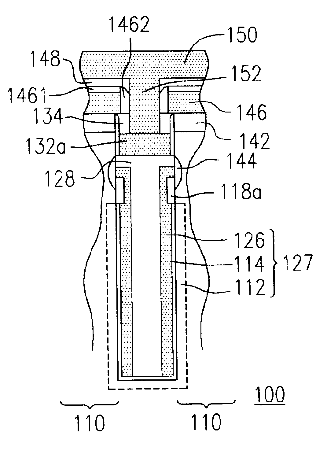
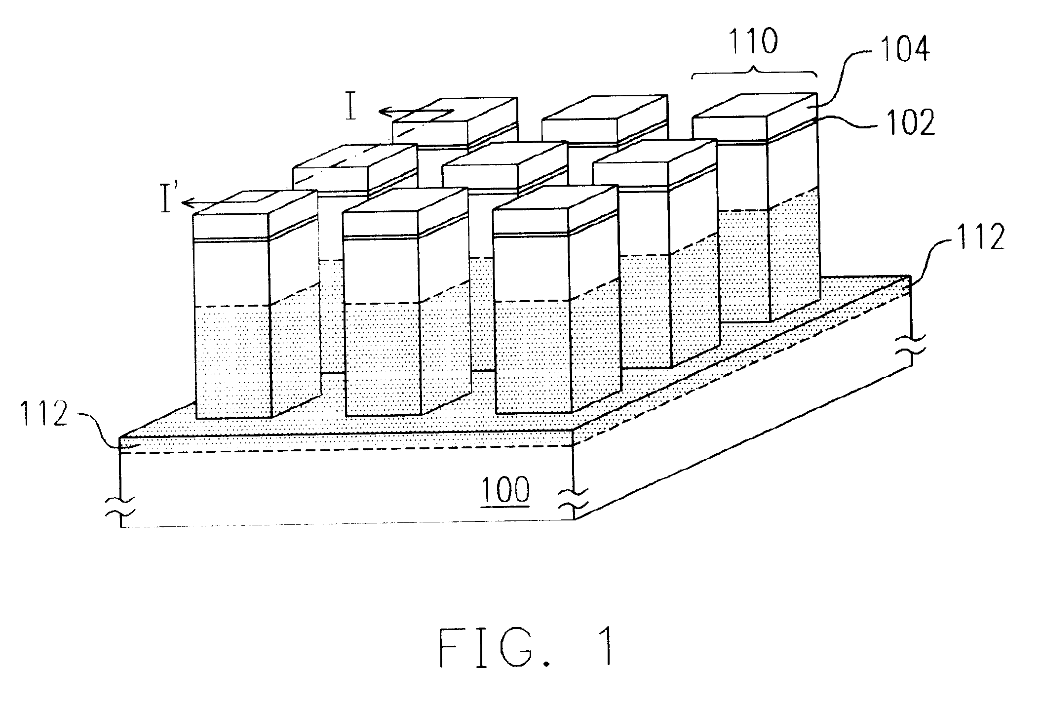
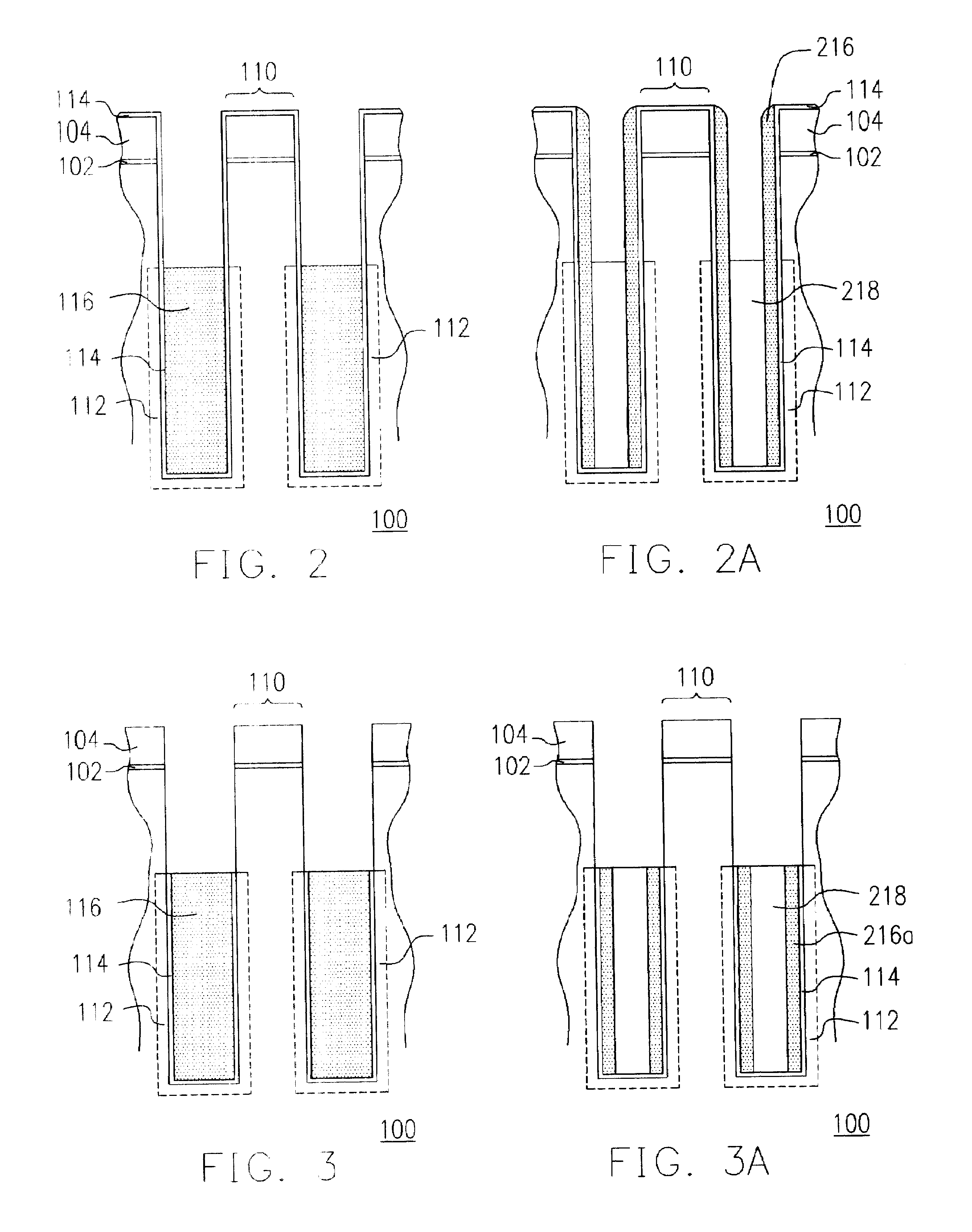
[0021]FIGS. 1–16 illustrate a process flow of fabricating a DRAM array according to a preferred embodiment of this invention. FIG. 1 clearly presents the array arrangement in a perspective view, FIGS. 2–9, 11–13 and 16(a) are cross-sectional view along line I—I″ in FIG. 1, while FIG. 16(b) is another cross-sectional view and FIGS. 10, 14 and 15 are top views.

[0022]More specifically, FIGS. 1–6 illustrate the process flow of forming the capacitors of the DRAM array, FIGS. 7–12 illustrate the process flow of forming the transistors of the DRAM array, and FIGS. 13–16 illustrate the subsequent steps including the fabrications of the bit lines and the word lines.

[0023]Fabrication of Capacitors

[0024]Referring to FIG. 1, a semiconductor substrate 100, such as a P-doped silicon substrate, is provided, and a pad oxide layer 102 and a patterned mask layer 104 are further formed on the substrate 100. The patterned mask layer 104 includes rows and columns of rectangular (or square) blocks, and i...


PUM


Abstract

A dynamic random access memory (DRAM) cell is described, including a semiconductor pillar on a substrate, a capacitor on a lower portion of a sidewall of the pillar, and a vertical transistor on an upper portion of the sidewall of the pillar. The vertical transistor includes a first doped region, a second doped region, a gate and a gate insulating layer. The first doped region is located in the sidewall and is coupled with the capacitor. The second doped region is located in a top portion of the pillar. The gate is disposed on the sidewall of the pillar between the first and the second doped regions, and the gate insulating layer is disposed between the sidewall and the gate.

Description

CROSS REFERENCE TO RELATED APPLICATIONS[0001]The present application is a continuation-in-part (CIP) application of U.S. patent application Ser. No. 10 / 210,031 filed Aug. 2, 2002 now U.S. Pat. No. 6,875,653, the entire contents thereof are incorporated herein for reference.BACKGROUND OF INVENTION[0002]1. Field of the Invention[0003]This invention pertains in general to semiconductor devices, and, more particularly, to memory cells for a dynamic random access memory (DRAM) and processes for manufacturing the same.[0004]2. Description of the Related Art[0005]In the semiconductor industry, DRAM is one of the most important integrated circuits, which motivates continuing research and development. There is a continuing effort to increase the storage capacity, improve the writing and reading speed, and decrease the device dimensions of a DRAM cell. A DRAM cell generally includes a transistor and a capacitor operated by the transistor. Conventionally, the design of a DRAM cell can be divid...

Claims


Application Information

Patent Timeline
IPC IPC(8): H01L21/8242H01L21/336H01L21/8238H01L21/8244H01L27/108H01L29/76H01L29/94
CPCH01L27/10832H01L27/10841H01L29/945H01L27/10864H01L27/10867H01L27/10888H01L27/10861H01L27/0207H10B12/373H10B12/395H10B12/0383H10B12/0385H10B12/038H10B12/485
Inventor WANG, TING-SHING
Owner PROMOS TECH INC
Why Eureka
Try Eureka