Organic n-channel semiconductor device of N,N' 3,4,9,10 perylene tetracarboxylic diimide

a technology of tetracarboxylic diimide and organic n-channel semiconductors, which is applied in the direction of thermoelectric device junction materials, semiconductor devices, electrical apparatus, etc., to achieve the effects of improved mobilities and current on/off, significant volatility, and high mobilities

Inactive Publication Date: 2006-04-11
GLOBALFOUNDRIES US INC
View PDF8 Cites 26 Cited by
  • Summary
  • Abstract
  • Description
  • Claims
  • Application Information

AI Technical Summary

Problems solved by technology

Only a limited number of materials have been developed thus far in the art for the n-type component of organic complementary circuitry.

Method used


Image

  • Organic n-channel semiconductor device of N,N' 3,4,9,10 perylene tetracarboxylic diimide
  • Organic n-channel semiconductor device of N,N' 3,4,9,10 perylene tetracarboxylic diimide
  • Organic n-channel semiconductor device of N,N' 3,4,9,10 perylene tetracarboxylic diimide

Examples


example 1

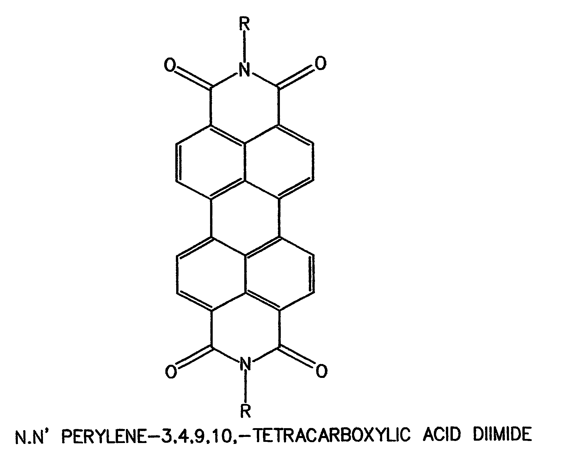
[0031]For N,N′ perylene 3,4,9,10 tetracarboxylic acid diimide, the mobility calculated in the saturation region was between 0.1 and 0.6 cm2 / Vs, with an on / off ratio of 10000 to 100000 the gate voltage being scanned from 100 to 0 V, with measurement under a nitrogen atmosphere. The devices are exposed to air prior to testing.

[0032]The invention provides an improvement over the present state of the art where contact imperfections are considered to be detrimental to device mobility.

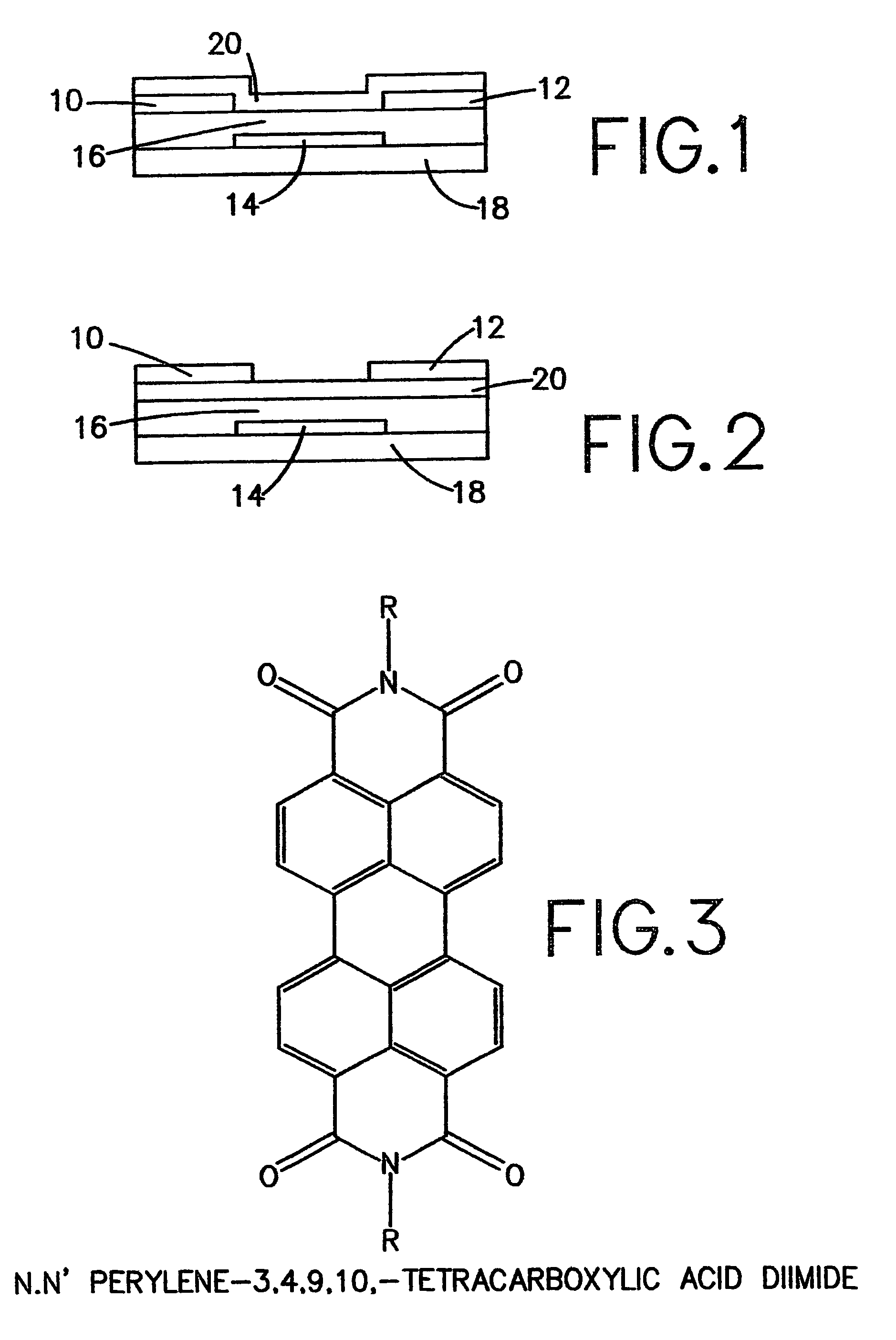
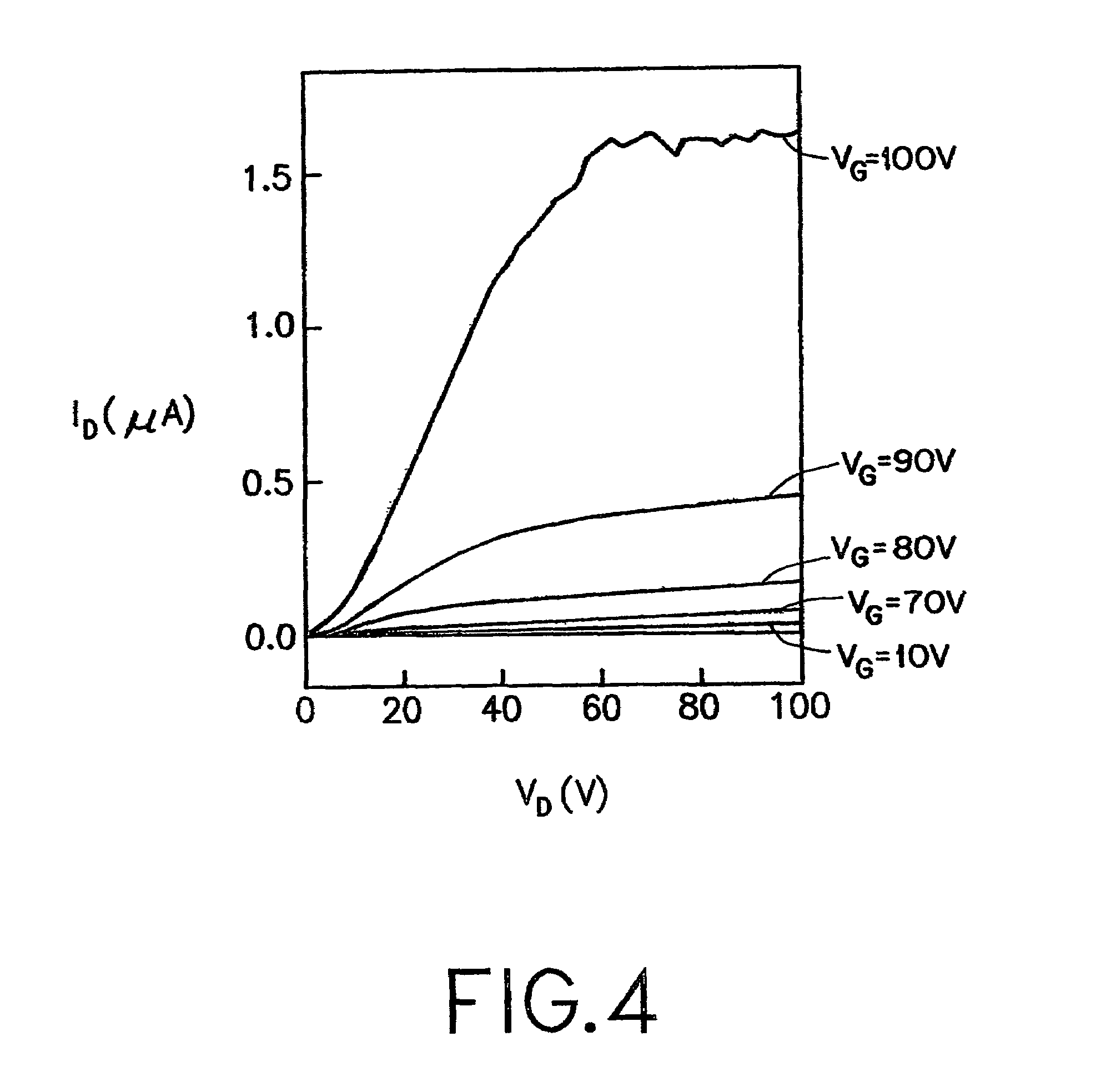
[0033]In FIGS. 4 and 5 data on a device is illustrated that has a N,N′ perylene 3,4,9,10 tetracarboxylic acid diimide as the semiconducting layer, a heavily doped Si wafer as gate electrode, a 500 nm thick, thermally grown SiO2 layer as the gate insulator, and Au source and drain electrodes deposited on the gate insulator corresponding to the bottom contact configuration that is depicted in FIG. 1. The channel length L of this device is 95 μm and the channel width W is 1500 μm.

[0034]The graph of FIG. 4 shows...


PUM


Abstract

The invention provides a device comprising an improved n-channel semiconducting film. This film consists of a perylene tetracaboxylic acid diimide compound and was deposited onto substrates by vacuum sublimation. Thin film transistor devices comprising such films as the semiconducting channel exhibit a field effect electron mobility greater than 0.01 cm2 / Vs and an on / off ratio of 10000 and higher.

Description

[0001]This non provisional application is a conversion of provisional patent application No. 60 / 288,692 filed May 4, 2001.FIELD OF THE INVENTION[0002]The invention is in the field of the plastic circuitry and components being employed in electronic technology, and in particular to devices containing N,N″ 3,4,9,10 perylene tetracarboxylic diimide semiconductor materials such devices as organic thin film transistors.BACKGROUND OF THE INVENTION[0003]The thin film transistor when made of organic materials in expected to become a key component of the plastic circuitry in display drivers of portable computers and pagers, and memory elements of transaction cards and identification tags, where ease of fabrication, mechanical flexibility, and moderate operating temperatures are important considerations.[0004]At the present state of the art there are circuitry situations such as with complimentary circuitry where properties unavailable in the present organic semiconductor materials such as th...

Claims


Application Information

Patent Timeline
Patent Type & Authority Patents(United States)
IPC IPC(8): H01L29/772H01L51/00H01L51/30H01L51/40
CPCH01L51/0053H01L51/001H01L51/0545H10K71/164H10K85/621H10K10/466
Inventor DIMITRAKOPOULOS, CHRISTOS DIMITRIOSGELORME, JEFFREY DONALDGRAHAM, TERESITA ORDONEZKOSBAR, LAURA LOUISEMALENFANT, PATRICK ROLAND LUCIEN
Owner GLOBALFOUNDRIES US INC
Why Eureka
Try Eureka