
Pixel structure

Active Publication Date: 2006-04-11
AU OPTRONICS CORP
View PDF3 Cites 12 Cited by
  • Summary
  • Abstract
  • Description
  • Claims
  • Application Information

AI Technical Summary

Benefits of technology

[0009]Accordingly, one object of the present invention is to provide a pixel structure that uses a short laser repair route for repairing any short-circuits between a scan line and a data line.
[0010]A second object of this invention is to provide a pixel structure that does not require any laser repair when there is any short-circuit between a scan line and a data line.

Problems solved by technology

Although the cathode ray tube (CRT) is economical to produce and has advantages in many aspects, possible production of hazardous radiation, a bulky body and enormous power consumption are three major factors that diminish its desirableness in a multi-terminal desktop environment.
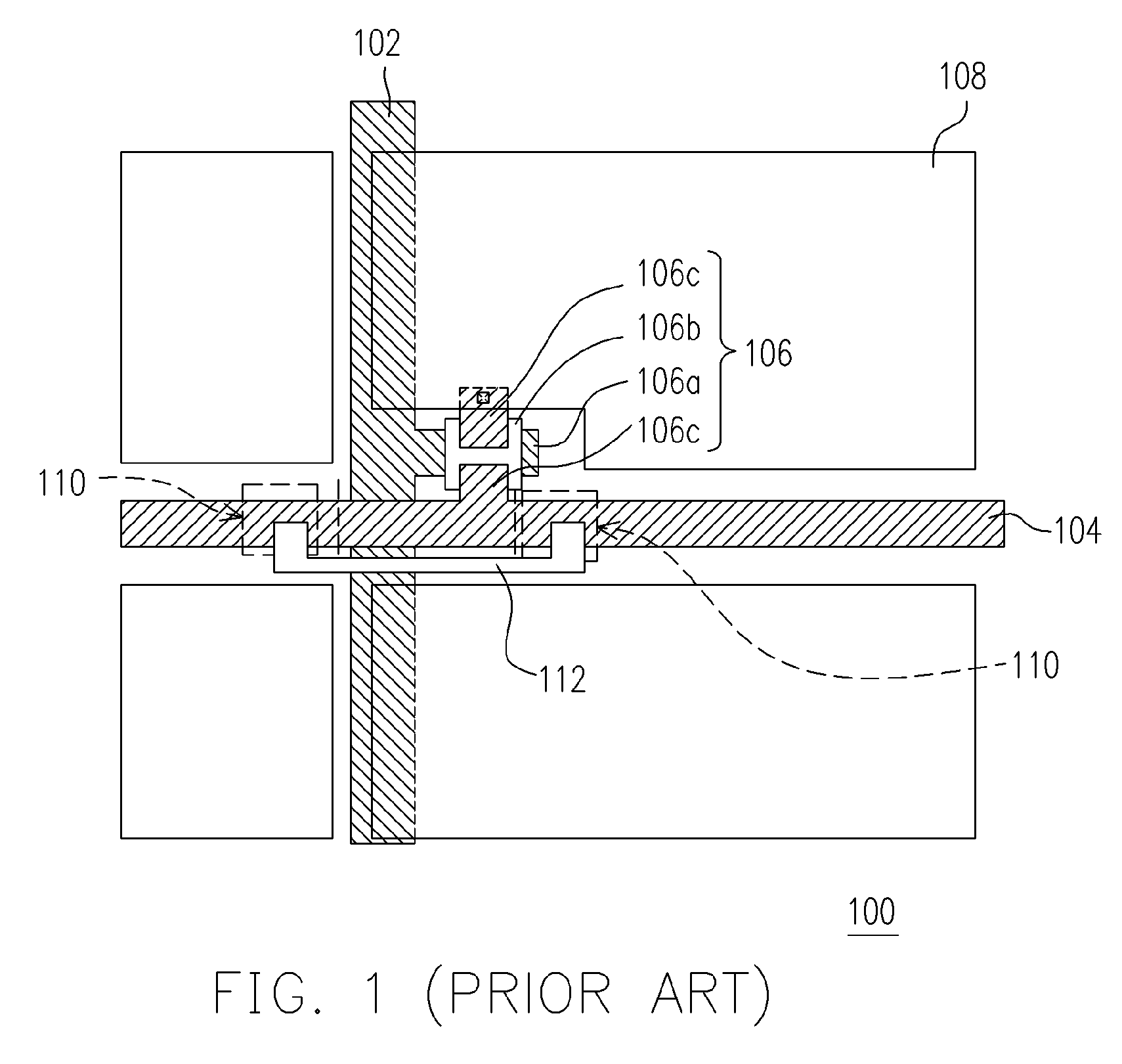
Thus, the thin metallic line 112 usually has a considerable length resulting in a longer and costlier repair.

Method used


Image

  • Pixel structure
  • Pixel structure
  • Pixel structure

Examples


first embodiment

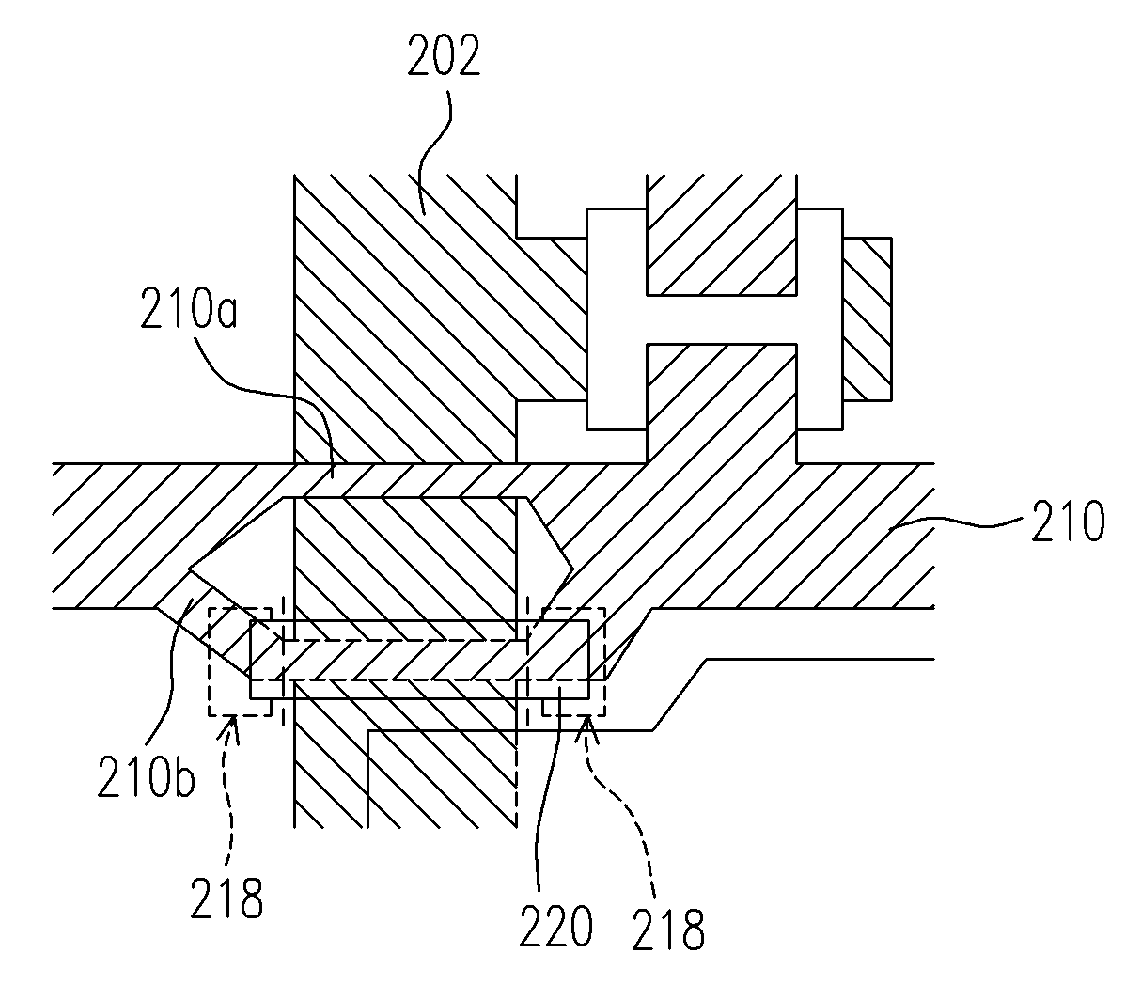
[0030]FIGS. 4 and 5 are schematic top views showing two processes for laser-repairing the pixel structure according to this invention. In FIG. 4, the data line 210 splits up into several subsidiary lines 210a, 210b (two lines in FIG. 4) in the area above the scan line 202. If one of the subsidiary lines 210b happens to have a short circuit with the scan line 202 due to defects caused by impurities or particles contamination, the short-circuited subsidiary line 210b is cut along the dashed line. Thereafter, a pair of repair openings 218 is formed in the second dielectric layer (not shown) and then a thin metallic layer 220 is formed between the repair openings 218 by performing a laser chemical vapor deposition (CVD) process. The thin metallic layer 220 reconnects the severed subsidiary line 210b together through the contact inside the repair openings 218.

[0031]However, those skilled in the art may notice that forming a thin metallic layer to reconnect the severed subsidiary data lin...

second embodiment

[0034]FIGS. 7 and 8 are schematic top views showing two processes for laser-repairing the pixel structure according to this invention. In FIG. 7, a first end 300a of the repair line 300 connects with the data line 210 but a second end 300b of the repair line 300 has no connection with the data line 210. If there is a short circuit between the scan line 202 and the data line 210, the section of the data line 210 having the short-circuiting is severed along the dashed lines. Thereafter, a repair opening 302 is formed at the second end 300b of the repair line. A thin metallic layer 304 is formed between the second end 300b of the repair line 300 and the data line 210 by performing a laser chemical vapor deposition (CVD) process. In other words, the thin metallic layer 304 reconnects the severed data line 210 through the repair line 300 and the thin metallic layer 304.

[0035]In FIG. 8, however, neither end of the repair line 300 has a direct connection with the data line 210. If there is...


PUM


Abstract

A pixel structure is provided. The pixel structure comprises a scan line, a data line, a pixel electrode and a thin film transistor. The data line branches out into a plurality of subsidiary lines in the area above the scan line. If there is a short circuit between the scan line and the data line, the short circuit can be repaired by cutting the connections to one of the branching subsidiary lines. In one embodiment of this invention, a repair line is set up on one side of the data line such that a portion of the repair line crosses over the scan line. If there is a short circuit between the scan line and the data line, a laser repair operation can be carried out through the repair line.

Description

CROSS REFERENCE TO RELATED APPLICATIONS[0001]This application claims the priority benefit of Taiwan application serial no. 92107253, filed Mar. 31, 2003.BACKGROUND OF INVENTION[0002]1. Field of Invention[0003]The present invention relates to a pixel structure. More particularly, the present invention relates to a pixel structure having a mechanism for repairing possible shortcircuits between a scan line and a data line.[0004]2. Description of Related Art[0005]With the rapid advance in semiconductor technologies and man-machine interface designs, multi-media are now at the forefront of communication. In a multi-media world, displays are important devices. Although the cathode ray tube (CRT) is economical to produce and has advantages in many aspects, possible production of hazardous radiation, a bulky body and enormous power consumption are three major factors that diminish its desirableness in a multi-terminal desktop environment. With better resolution, space utilization and power ...

Claims


Application Information

Patent Timeline
IPC IPC(8): H01L29/04G02F1/136G02F1/1362H01L21/00H01L27/146H01L27/32
CPCG02F1/136259G02F2001/136263H01L2251/568H01L27/3297H01L27/14609G02F1/136263H10K59/131H10K71/861
Inventor LAI, HAN-CHUNG
Owner AU OPTRONICS CORP
Learn More