Patterning of surfaces utilizing microfluidic stamps including three-dimensionally arrayed channel networks

a microfluidic and channel network technology, applied in the direction of fluid speed measurement, immobilised enzymes, chemical vapor deposition coating, etc., can solve the problems of complex channel network complex systems that require more complex connectivity than can be generated, difficult to perform, and high cos

Inactive Publication Date: 2007-09-11
PRESIDENT & FELLOWS OF HARVARD COLLEGE
View PDF25 Cites 81 Cited by
  • Summary
  • Abstract
  • Description
  • Claims
  • Application Information

AI Technical Summary

Benefits of technology

[0007]The present invention involves, in certain embodiments, improved microfluidic systems and procedures for fabricating improved microfluidic systems, which contain one or more levels of microfluidic channels. The inventive methods can provide a convenient route to topologically complex and improved microfluidic systems. The present invention also, in some embodiments, involves microfluidic systems and methods for fabricating complex patterns of materials, such as biological materials and cells, on surfaces. In such embodiments, the invention involves microfluid...

Problems solved by technology

The need for complexity in microfluidic systems is increasing rapidly as sophisticated functions—chemical reactions and analyses, bioassays, high-throughput screens, and sensors—are being integrated into single microfluidic devices.
Complex systems of channels require more complex connectivity than can be generated in conventional two-dimensional microfluidic systems having a single leve...

Method used


Image

  • Patterning of surfaces utilizing microfluidic stamps including three-dimensionally arrayed channel networks
  • Patterning of surfaces utilizing microfluidic stamps including three-dimensionally arrayed channel networks
  • Patterning of surfaces utilizing microfluidic stamps including three-dimensionally arrayed channel networks

Examples


example 1

Fabrication of a Mold Master by Multi-Level Photolithography

[0168]A mold master of photoresist on silicon having two levels of features in positive, high relief (i.e., protruding above the surface of the silicon wafer) was fabricated using the two-level photolithography technique outlined in FIG. 8. Designs for the channel systems for the first and second levels were generated with a CAD computer program (Free-Hand 8.0, MacroMedia, San Francisco, Calif.). High resolution (3386 dpi) transparencies were made by printing with a commercial printer (Linotype, Hercules Computer Technology, Inc., Freemont, Calif.) from the CAD computer files. Two transparencies were produced, the first comprising the photomask for producing features in the first level of the mold master and the second comprising photomask for producing the features in the second level of the mold master.

[0169]Negative photoresist (SU8-50, Microlithography Chemical Corp., Newton, Mass.) was spin-coated (at about 5,000 rpm f...

example 2

Fabrication of a Three-Dimensional Microfluidic Network Including a System of Channels in a “Basketweave” Configuration

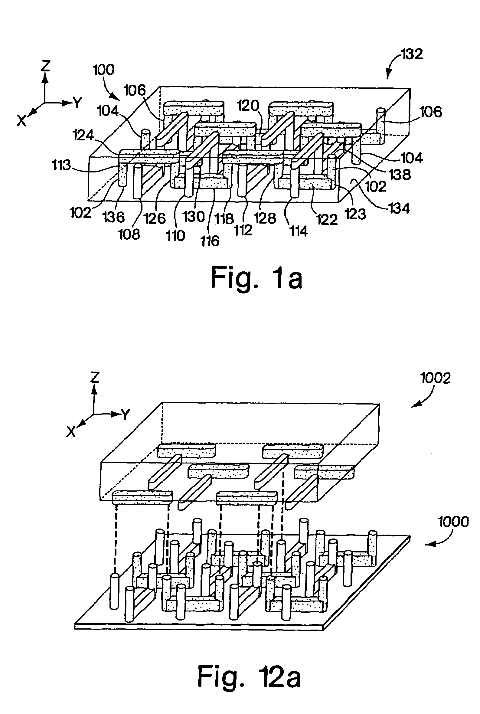
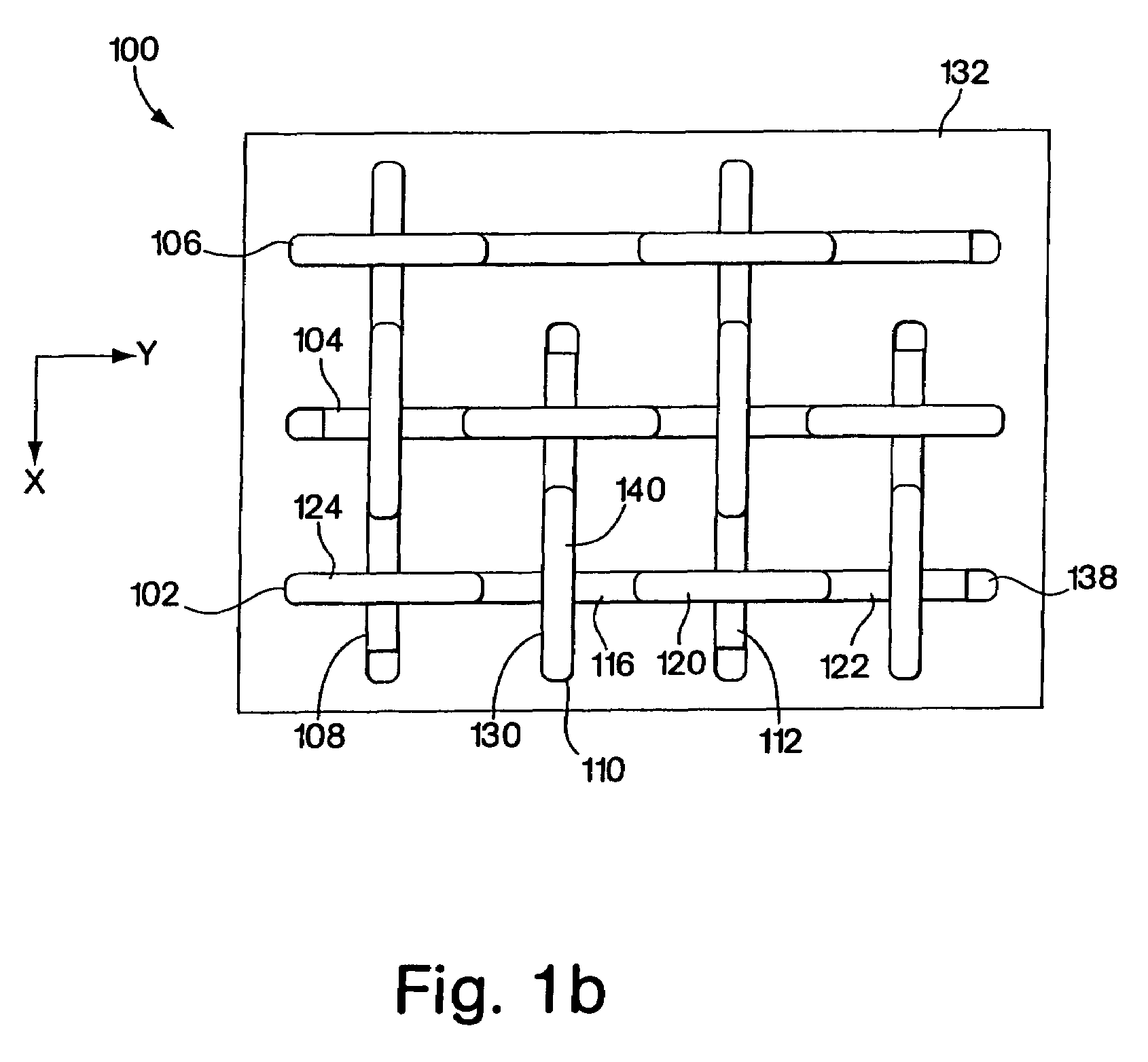
[0172]In the following example, the method outlined in FIGS. 9a and 9b was utilized to produce a microfluidic network structure including a channel pattern therein having a basketweave structure similar to that illustrated in FIG. 1a. First, a bottom master was produced as described above in Example 1 having disposed thereon two-level topological features for forming channels within the molded replica arranged similarly to those shown schematically in FIG. 12a by bottom master 1000. The second step of the process comprised formation of a top master including features for forming channels in the uppermost level of the replica molded membrane. A similar schematic arrangement of features for producing the channels, and the way in which the channels of the upper mold master and lower mold master fit together to mold the overall structure, is also illustrated in FIG. 12a...

example 3

Fabrication of Microstructures by Replica Molding With a Microfluidic Network Structure

[0179]A microfluidic membrane including a three-level channel system in a basketweave pattern was produced as described in Example 2. The microfluidic membrane was placed upon a flat PDMS slab so that the upper surface of the PDMS slab and the lower surface of the membrane were in conformal contact but were not irreversibly sealed to each other. The upper surface of the membrane was left open to the atmosphere. An epoxy prepolymer (EP-TEK, Epoxy Technology, Billerica, Mass.) was then placed at the channel openings and allowed to fill the channel structure by capillary action. After approximately 1 hour standing at ambient pressure, the epoxy had degassed and filled the channels completely. The filled channels were then exposed to UV light (as described above in Example 1) for about 20 min through the PDMS. The surrounding PDMS microfluidic membrane was then dissolved in tetrabutylammonium fluoride...


PUM

PropertyMeasurementUnit
Elastomericaaaaaaaaaa
Adhesion strengthaaaaaaaaaa
Interactionaaaaaaaaaa

Abstract

The present invention describes improved microfluidic systems and procedures for fabricating improved microfluidic systems, which contain one or more levels of microfluidic channels. The methods for fabrication the systems disclosed can provide a convenient route to topologically complex and improved microfluidic systems. The microfluidic systems can include three-dimensionally arrayed networks of fluid flow paths therein including channels that cross over or under other channels of the network without physical intersection at the points of cross over. The microfluidic networks can be fabricated via replica molding processes utilizing mold masters including surfaces having topological features formed by photolithography. The present invention also involves microfluidic systems and methods for fabricating complex patterns of materials, such as biological materials and cells, on surfaces utilizing the microfluidic systems. Specifically, the invention provides microfluidic surface patterning systems and methods for fabricating complex, discontinuous patterns on surfaces that can incorporate or deposit multiple materials onto the surfaces. The present invention also provides improved microfluidic stamps or applicators for microcontact surface patterning, which are able to pattern onto a surface arbitrary two-dimensional patterns, and which are able to pattern multiple substances onto a surface without the need for multiple steps of registration or stamping during patterning and without the need to selectively “ink” different regions of the stamp with different materials.

Description

RELATED APPLICATIONS[0001]This application is a divisional of U.S. patent application Ser. No. 09 / 578,562, entitled “Patterning of Surfaces Utilizing Microfluidic Stamps Including Three-Dimensionally Arrayed Channel Networks,” filed on May 25, 2000 now U.S. Pat. No. 6,686,184, currently, which is herein incorporated by reference in its entirety.FEDERALLY SPONSORED RESEARCH[0002]This invention was made with government support: Grant Nos. GM51559; GM30367 from the National Institutes of Health, and Grant No. ECS9729405 from the National Science Foundation. The government has certain rights to the invention.FIELD OF INVENTION[0003]The present invention involves microfluidic network structures comprising microfluidic stamps and methods for using such stamps for forming patterns on surfaces.BACKGROUND OF THE INVENTION[0004]The need for complexity in microfluidic systems is increasing rapidly as sophisticated functions—chemical reactions and analyses, bioassays, high-throughput screens, a...

Claims


Application Information

Patent Timeline
IPC IPC(8): C12Q1/00C07K17/00C07K17/02C12M1/00C12N11/00C12N11/02B01F13/00B01L3/00B01L3/02B29C31/04B29C33/42B29C39/10B81B1/00B81C1/00C40B40/10C40B60/14G01N33/50
CPCB01L3/0258B01L3/0262B01L3/502707B29C39/10B81B1/00B81C99/009B82Y5/00B82Y30/00G01N33/5005B01F13/0059B01J2219/00382B01J2219/00527B01J2219/00585B01J2219/00596B01J2219/00605B01J2219/0061B01J2219/0063B01J2219/00637B01J2219/00659B01J2219/0072B01J2219/00725B01J2219/00743B01L2200/12B01L2300/0816B01L2300/0861B01L2300/0874B01L2300/0887B29C31/04B29C33/424C40B40/10C40B60/14Y10S530/812Y10S530/81Y10S530/815Y10S530/811B33Y80/00B01F33/30C12N11/00
Inventor ANDERSON, JANELLE R.CHIU, DANIEL T.JEON, NOO LIHUANG, SUIKANE, RAVINDRACHOI, INSUNG S.INGBER, DONALD E.WHITESIDES, GEORGE M.
Owner PRESIDENT & FELLOWS OF HARVARD COLLEGE
Why Eureka
Try Eureka