Etching methods and apparatus for producing semiconductor devices

Inactive Publication Date: 2006-04-18
KAWASAKI MICROELECTRONICS
View PDF15 Cites 15 Cited by
  • Summary
  • Abstract
  • Description
  • Claims
  • Application Information

AI Technical Summary

Benefits of technology

[0013]It is an object of this invention to provide methods and apparatus for producing semiconductor devices with an increased production effic

Problems solved by technology

When the step is changed from the BARC etching to the WSi etching, a total gas flow rate significantly changes due to termination of the Ar gas flow, and a total gas pressure in the chamber may become unstable.
The total pressure and the ratio between component gases in the process gas may become unstable due to an abrupt increase of HBr gas flow rate.
When the step is changed from the poly-Si etching to the overetching, the total gas pressure may become unstable because the total pressure of the overetching process gas is significantly higher than that of the main etching process gas.
The downtime for the temporary interruption of the plasma discharge signi

Method used


Image

  • Etching methods and apparatus for producing semiconductor devices
  • Etching methods and apparatus for producing semiconductor devices
  • Etching methods and apparatus for producing semiconductor devices

Examples


Example

EXAMPLE 1

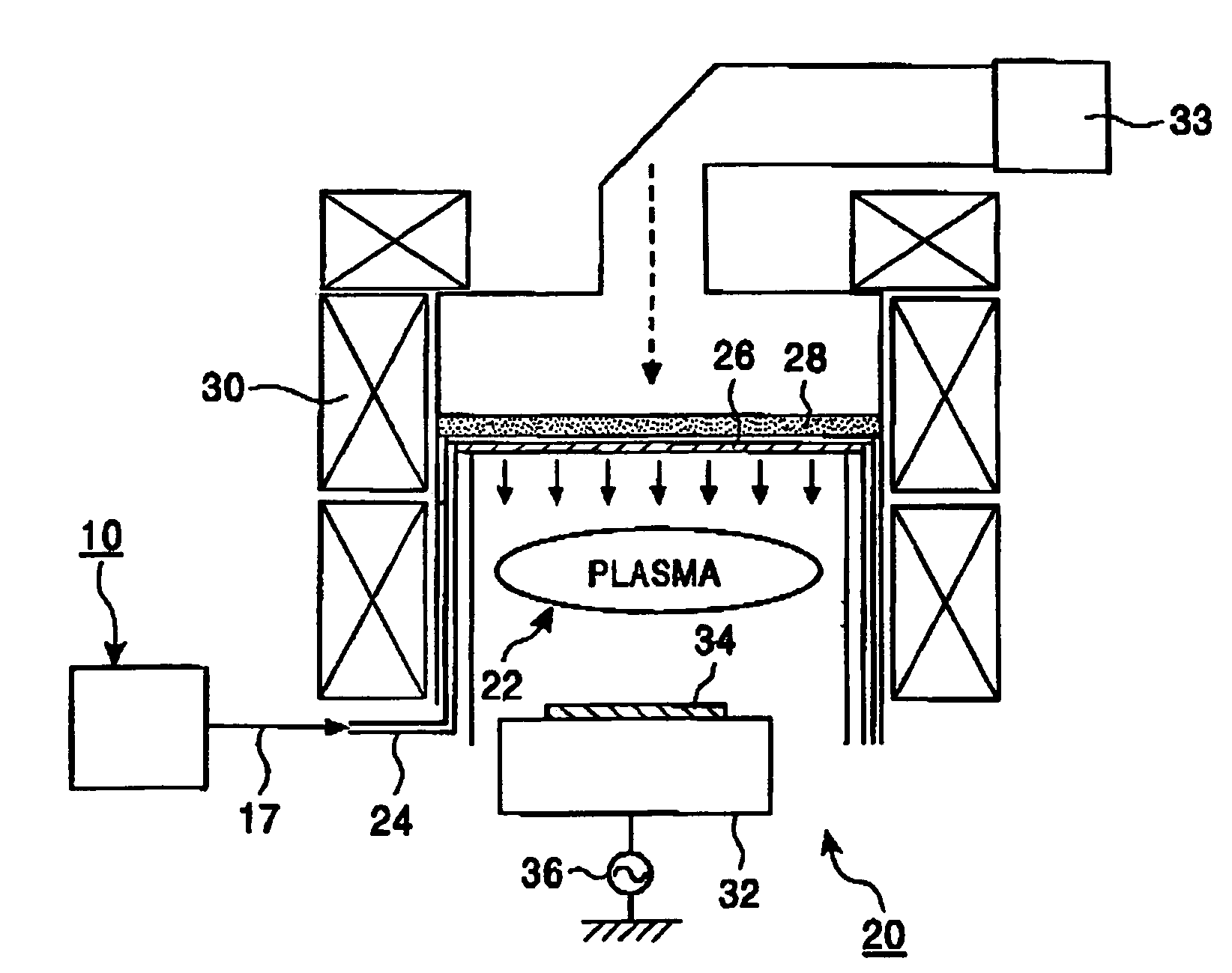
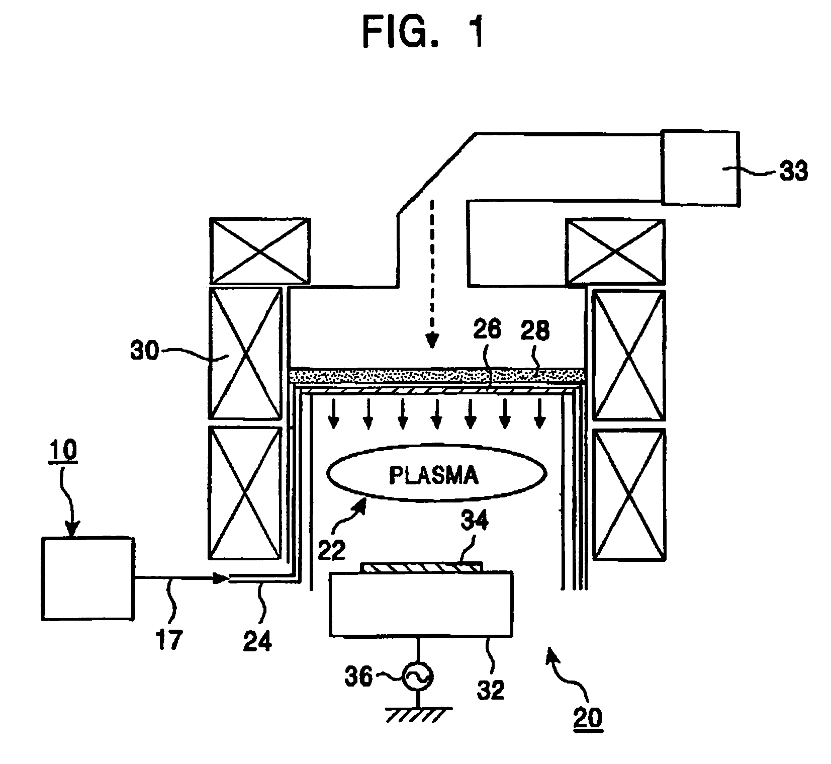
[0089]Semiconductor substrates each having a multi-layered structure of BARC / WSi / poly-Si / SiO2 / Si-substrate were prepared and etched in an ECR etching chamber by supplying process gases composed of component gases with flow rates shown in TABLE 1. The process gases are continuously excited by a plasma discharge without an interruption throughout the entire steps of BARC etching, WSi etching, poly-Si main etching, and poly-Si overetching. In TABLE I, a hyphen (-) indicates that the corresponding component gas was not used. Other etching conditions including the total gas pressure, the microwave power, and the RF power are summarized in TABLE 2. The process time required for etching the BARC (110 nm) / WSi (100 nm) / poly-Si (150 nm) layers per substrate are shown in TABLE 3. The etching time for each layer was determined by automatic end-point detection, while the overetching time was fixed to thirty seconds.

Example

Comparative Example 1

[0090]Semiconductor substrates were prepared in the same manner as in Example 1 and etched in the same etching chamber while supplying process gases including component gases with flow rates shown in TABLE 1. The plasma discharge was interrupted each time when the etching step was changed. A fifteen seconds switching time was provided to stabilize the process gas in the chamber for each time of changing the step. The process times required for etching the BARC (110 nm) / WSi (100 nm) / poly-Si (150 nm) layers per substrate are shown in TABLE 2.

[0091]TABLE 1ComponentStep / Flow Rate (sccm)GasBARCWSipoly-SiOveretchingExample 1Cl220140 80—HBr2020100 150O23020 5 5Ar50———ComparativeCl2208080—Example 1HBr——100 150O220 8 5 5Ar100 ———

[0092]TABLE 2Step / ValueConditionsBARCWSipoly-SiOveretchingExample 1Pressure (Pa)1.00.40.41.2Microwave600400400400Power (W)RF Power20302525(W)ComparativePressure (Pa)1.00.30.41.2Example 1Microwave600400400400Power (W)RF Power15252525(W)

[0093]TABLE...

Example

EXAMPLE 2

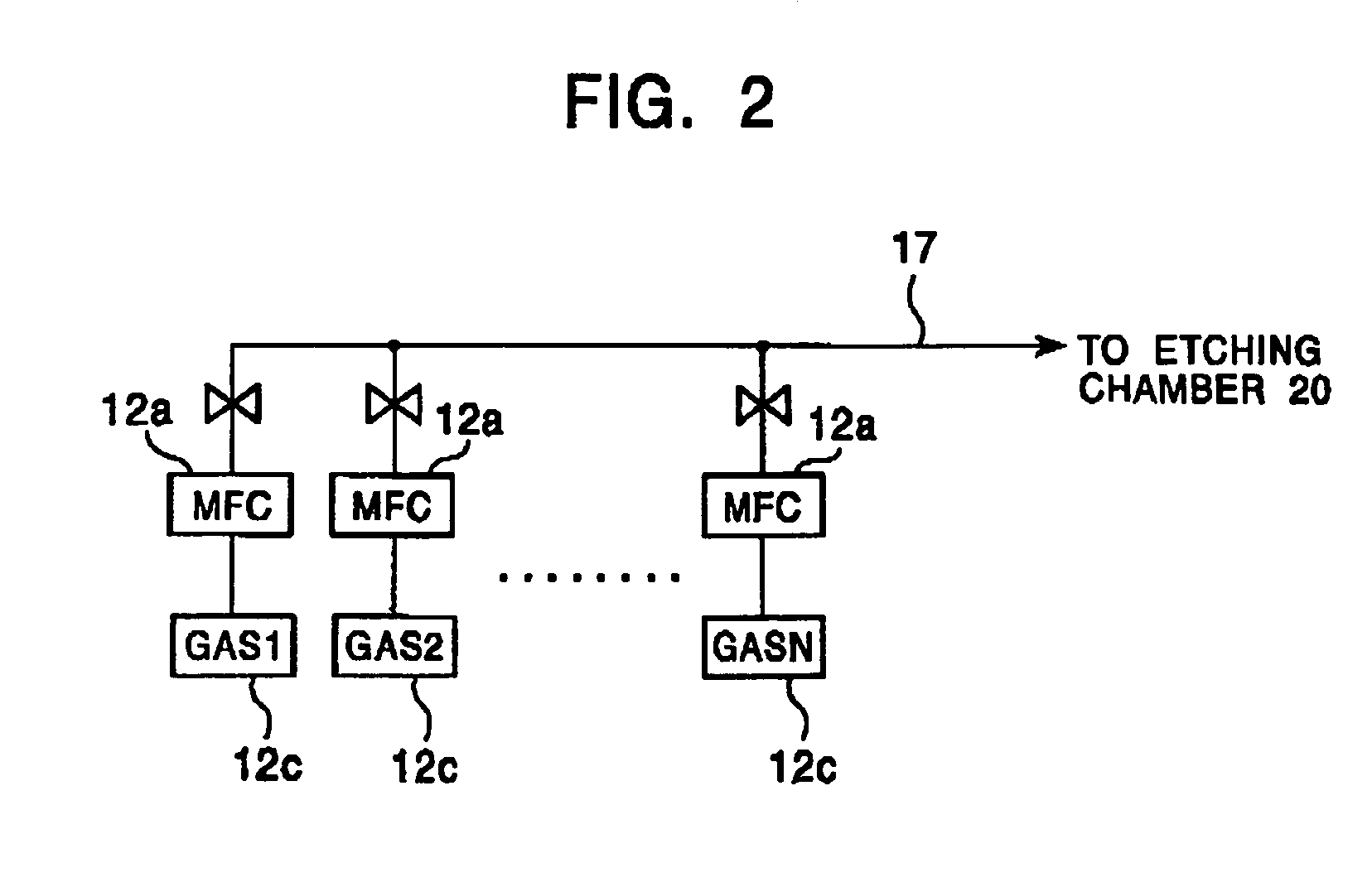
[0100]Semiconductor device substrates each having a multi-layered structure of BARC / SiO2 / WSi / poly-Si on SiO2 / Si-substrate are etched in an ECR etching chamber by a completely continuous plasma excitation without an interruption using process gases shown in TABLE 4. Other conditions are summarized in TABLE 5. The conditions in other steps are the same as shown in TABLE 2. Some of the process gases are preliminarily prepared according to the ratios shown in TABLE 4 and reserved in the gas reservoir, and are supplied from the gas reservoir to the etching chamber. In TABLE 4, the hyphen (-) indicates that the corresponding component gas is not used. The process times for etching the BARC (110 nm) / SiO2 (100 nm) / WSi (100 nm) / poly-Si (150 nm) layers per wafer are shown in TABLE 4.


PUM


Abstract

A multi-layered film on a semiconductor substrate is etched with a multi-step etching process by sequentially providing a plurality of process gases having different compositions in a chamber. A plasma discharge to excite the process gases is continued without an interruption during a switch to a different process gas. A relationship between different process gases desirable for the continuous plasma excitation is also disclosed. An apparatus suitable to practice this continuous plasma excitation process includes a process gas supply system having a gas reservoir. A mixture of at least two component gases is prepared and reserved in the reservoir, and is supplied to the etching chamber when it is needed.

Description

BACKGROUND OF THE INVENTION[0001]1. Field of Invention[0002]This invention relates to methods and apparatus for making semiconductor devices. In particular, this invention relates to etching processes and etching apparatus.[0003]2. Description of the Related Art[0004]In etching processes for producing semiconductor devices, a film formed on a surface of a semiconductor substrate (wafer) is etched through a mask pattern formed on the film by a chemical reaction. Etching processes are classified into dry processes and wet processes. In dry processes, a process gas introduced into an etching chamber is excited by a plasma generated by an electric discharge, and a surface of a masked semiconductor substrate is exposed to the plasma to etch the film on the substrate. The process gas provided in the etching chamber is a gaseous mixture, which is formulated depending on the material of the film to be etched.[0005]In a conventional process, for example, a process gas is introduced into an e...

Claims


Application Information

Patent Timeline
IPC IPC(8): H01L21/20H01L21/3065H01L21/302H01L21/311H01L21/3213
CPCH01L21/31116H01L21/32137H01L21/32136H01L21/31138
Inventor SUZUKI, KOJI
Owner KAWASAKI MICROELECTRONICS
Why Eureka
Try Eureka