Four phase charge pump operable without phase overlap with improved efficiency

a four-phase charge and efficiency technology, applied in the field of electric circuits, can solve the problems of reducing the effective series resistance of capacitors, limiting the size of capacitors in integrated circuits, and increasing frequency will not improve pump performance, so as to facilitate the conductance of transistors and increase clock frequency

Active Publication Date: 2006-04-18
SANDISK TECH LLC
View PDF9 Cites 134 Cited by
  • Summary
  • Abstract
  • Description
  • Claims
  • Application Information

AI Technical Summary

Benefits of technology

[0013]Clock frequency can be increased by providing with each parallel tansistor a pre-charge diode to pre-charge the gate of the parallel transistor after the input node charge is raised but before the charge transfer. This facilitates the conductance of the transistor with each transistor cycle.

Problems solved by technology

While increasing capacitor charge reduces effective series resistance, Rs, there is a practical limitation of capacitor size in an integrated circuit.
While clock frequency, fosc, reduces series resistance, the charge must be able to be transferred from node to node within a cycle, otherwise increasing frequency will not improve pump performance.

Method used


Image

  • Four phase charge pump operable without phase overlap with improved efficiency
  • Four phase charge pump operable without phase overlap with improved efficiency
  • Four phase charge pump operable without phase overlap with improved efficiency

Examples


Embodiment Construction

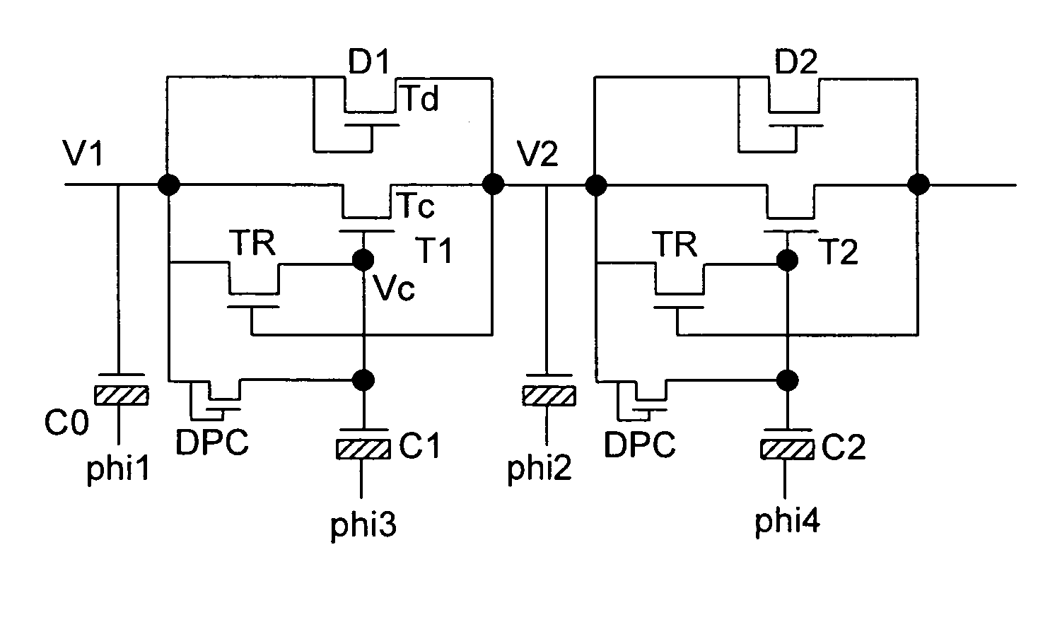
[0020]FIG. 3 is a schematic of a charge pump in accordance with one embodiment of the invention in which the cells of the conventional Dickson charge pump are modified to facilitate charge transfer and to accommodate a higher clock frequency or fosc. FIG. 3 shows two adjacent cells, such as diodes D1 and D2 of the Dickson charge pump of FIG. 1, for transferring charge from node V1 to node V2. Each cell is modified by providing a MOS transistor T1 or T2 in parallel with diode D1 or diode D2 which facilitate the transfer of residual trapped charge at each node. A recovery transistor TR is connected between the gate of transistor T1 and node V1 with the gate of transistor TR controlled by the voltage on node V2. When charge is transferred from node V1 to node V2, the increased voltage at node V2 causes transistor TR to conduct and bring the voltage on the gate of transistor T1 to the voltage level of node V1. After clock φ3 is removed, the conductance of transistor T1 is terminated.

[00...


PUM


Abstract

In a Dickson type charge pump in which a plurality of serially connected diodes sequentially respond to anti-phase 50 / 50 clock cross over or overlapped (φ1, φ2), efficiency of the charge pump is increased by providing with each diode a charge transfer transistor in parallel therewith between two adjacent nodes, and driving the charge transfer transistor to conduction during a time when the parallel diode is conducting thereby transferring any residual trapped charge at one node through the charge transfer transistor to the next node. Operating frequency can be increased by providing a pre-charge diode coupling an input node to the gate of the charge transfer transistor to facilitate conductance of the charge transfer transistor, and by coupling the control terminal of the charge transfer transistor to an input node in response to charge on an output node to thereby equalize charge on the control terminal and on the input node during a recovery period.

Description

BACKGROUND OF THE INVENTION[0001]This invention relates generally to electric circuits that generate a voltage larger than a supply voltage from which they operate by the switching of charge along serial capacitive cells, known as charge pumps.[0002]A well known charge pump is the Dickson charge pump, which is shown in FIG. 1. As described by Louie Pylarinos of the University of Toronto in “Charge Pumps: An Overview”, the circuit has two pumping clocks which are anti-phased and have a voltage amplitude of Vφ or {overscore (Vφ)}. Serial diodes or diode connected NMOSFETS, D1–D4, operate as self-timed switches characterized by a forward biased voltage, Vt, which is the threshold voltage of each diode. Each diode has a stray capacitance, Cs, associated therewith. The charge pump operates by pumping charge along the diode chain as capacitors C1–C4 are successively charged and discharged during each clock cycle. For example, when Vφ goes high, diode D1 conducts and the voltage at its ano...

Claims


Application Information

Patent Timeline
Patent Type & Authority Patents(United States)
IPC IPC(8): G05F3/02G05F1/10H02M3/07
CPCH02M3/073H02M2003/078H02M2003/075H02M3/075H02M3/078
Inventor PAN, FENGPHAM, TRUNG
Owner SANDISK TECH LLC
Why Eureka
Try Eureka