Generating a library of simulated-diffraction signals and hypothetical profiles of periodic gratings

a technology of periodic gratings and hypothetical profiles, applied in the field of wafer metrology, can solve the problems of limiting the size and resolution of the hypothetical diffraction signal library that can be generated, time and computational capacity needed to generate hypothetical diffraction signals, and the number of entries and the increment between entries

Active Publication Date: 2006-04-18
TOKYO ELECTRON US HOLDINGS INC
View PDF10 Cites 43 Cited by
  • Summary
  • Abstract
  • Description
  • Claims
  • Application Information

AI Technical Summary

Problems solved by technology

In general, the process of generating a hypothetical-diffraction signal involves performing a large number of complex calculations, which can be time and computationally intensive.
The amount of time and computational capability and capacity needed to generate hypothetical-diffraction signals can limit the size and resolution (i.e., the number of entries and the increment between entries) of the library of hypothetical-diffraction signals that can be generated.

Method used


Image

  • Generating a library of simulated-diffraction signals and hypothetical profiles of periodic gratings
  • Generating a library of simulated-diffraction signals and hypothetical profiles of periodic gratings
  • Generating a library of simulated-diffraction signals and hypothetical profiles of periodic gratings

Examples


Embodiment Construction

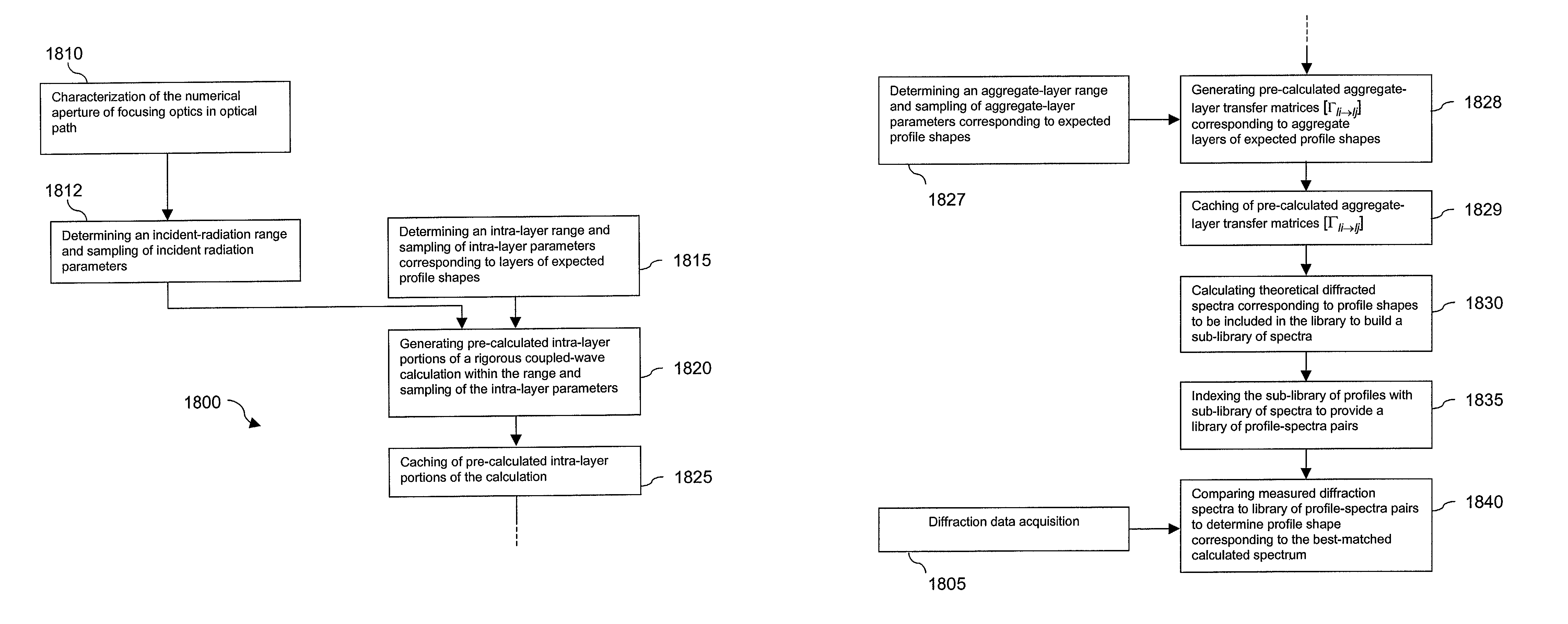
[0027]The following description sets forth numerous specific configurations, parameters, and the like. It should be recognized, however, that such description is not intended as a limitation on the scope of the present invention, but is instead provided as a description of exemplary embodiments.

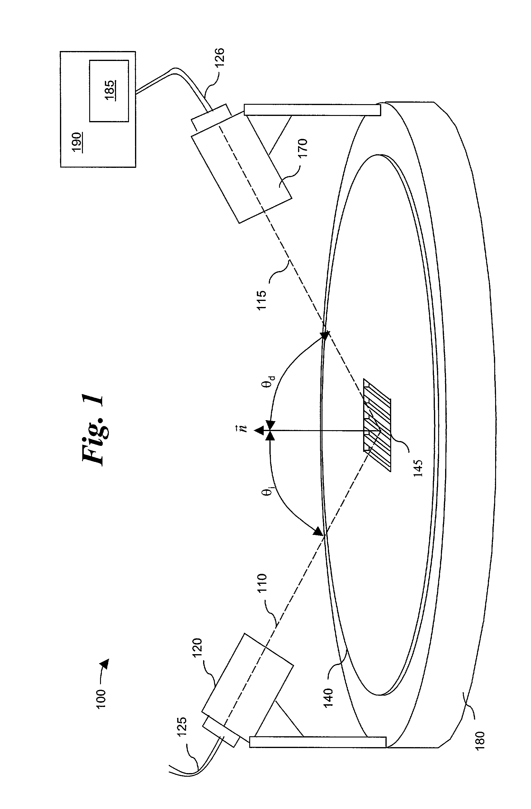
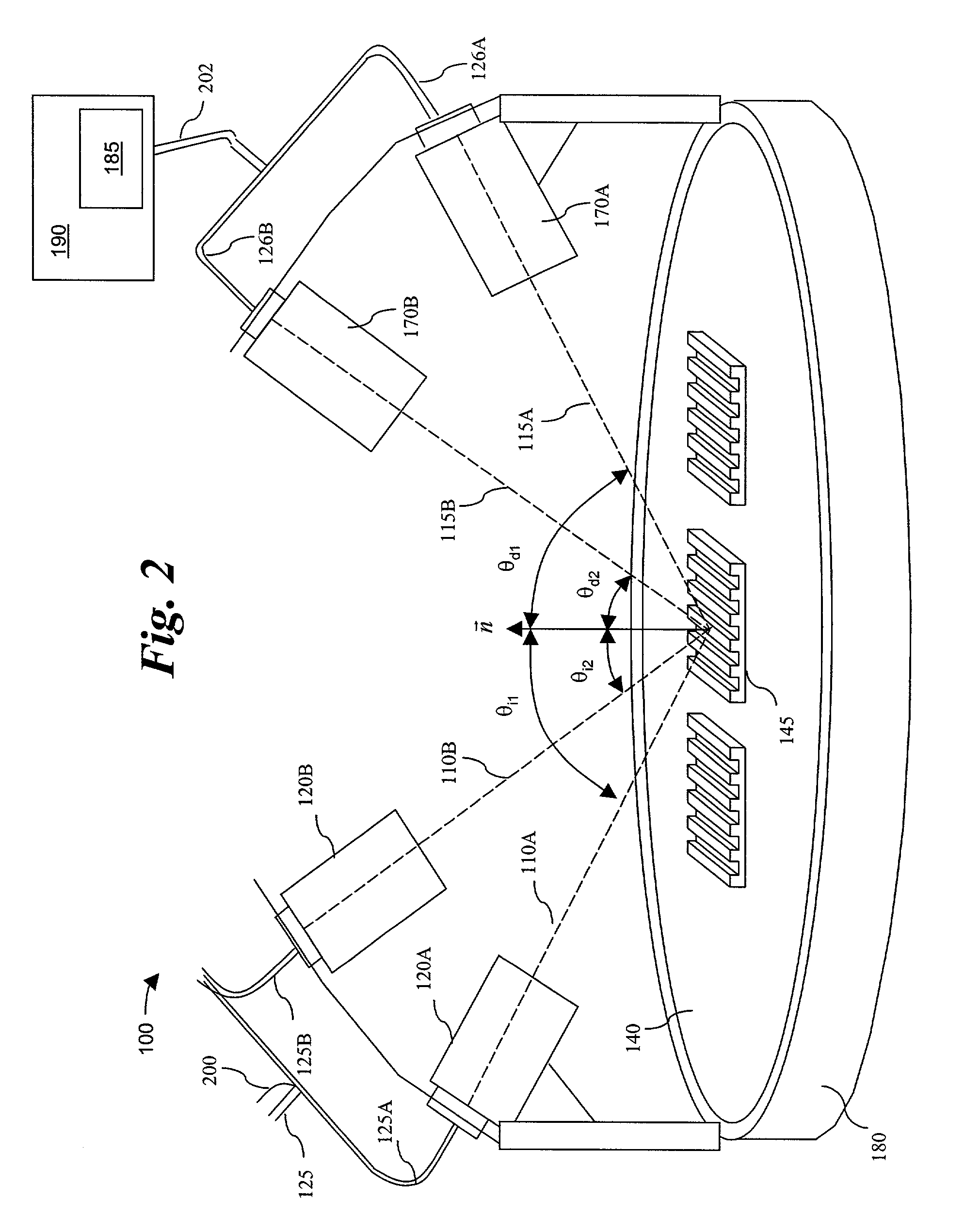
[0028]With reference to FIG. 1, a periodic grating 145 is depicted on a semiconductor wafer 140. As depicted in FIG. 1, wafer 140 is disposed on a process plate 180, which can include a chill plate, a hot plate, a developer module, and the like. Alternatively, wafer 140 can also be disposed on a wafer track, in the end chamber of an etcher, in an end-station or metrology station, in a chemical mechanical polishing tool, and the like.

[0029]As described earlier, periodic grating 145 can be formed in test areas on wafer 140 that are proximate to or within an operating structure formed on wafer 140. For example, periodic grating 145 can be formed adjacent to a device formed on wafer 140. Alternat...


PUM

PropertyMeasurementUnit
angle of incidence θiaaaaaaaaaa

Abstract

A library of simulated-diffraction signals and hypothetical profiles of a periodic grating can be generated by generating diffraction calculations for a plurality of blocks of hypothetical layers. A diffraction calculation for a block of hypothetical layers characterizes, in part, the behavior of a diffraction beam in the block of hypothetical layers. Each block of hypothetical layers includes two or more hypothetical layers, and each hypothetical layer characterizes a layer within a hypothetical profile. The diffraction calculations for the blocks of hypothetical layers are stored prior to generating the library. The simulated-diffraction signals to be stored in the library are then generated based on the stored diffraction calculations for the blocks of hypothetical layers.

Description

BACKGROUND[0001]1. Field of the Invention[0002]The present invention relates to wafer metrology, and more particularly to generating a library of simulated-diffraction signals for use in optical metrology to determine the profile of periodic gratings.[0003]2. Related Art[0004]In semiconductor manufacturing, periodic gratings are typically utilized for quality assurance. For example, one typical use of such periodic gratings includes fabricating a periodic grating in proximity to the operating structure of a semiconductor chip. By determining the profile of the periodic grating, the quality of the fabrication process utilized to form the periodic grating, and by extension the semiconductor chip proximate the periodic grating, can be evaluated.[0005]Optical metrology can be utilized to determine the profile of a periodic grating. In general optical metrology involves directing an incident beam at the periodic grating, and measuring the resulting diffraction beam. The characteristics o...

Claims


Application Information

Patent Timeline
Patent Type & Authority Patents(United States)
IPC IPC(8): G06G7/48G01B11/00G01N21/47G01N21/956
CPCG01B11/00G01N21/956G01N21/4788
Inventor NIU, XINHUIJAKATDAR, NICKHIL
Owner TOKYO ELECTRON US HOLDINGS INC
Why Eureka
Try Eureka