

Flip chip interconnection structure
a technology of interconnection structure and flip chip, which is applied in the direction of semiconductor/solid-state device details, manufacturing tools, transportation and packaging, etc., can solve the problems of limited long-term reliability and difficulty in reducing the pitch of interconnection, and achieve low yield strength and high elongation to failure
- Summary
- Abstract
- Description
- Claims
- Application Information
AI Technical Summary
Benefits of technology
Problems solved by technology
Method used
Image

Examples
second embodiment
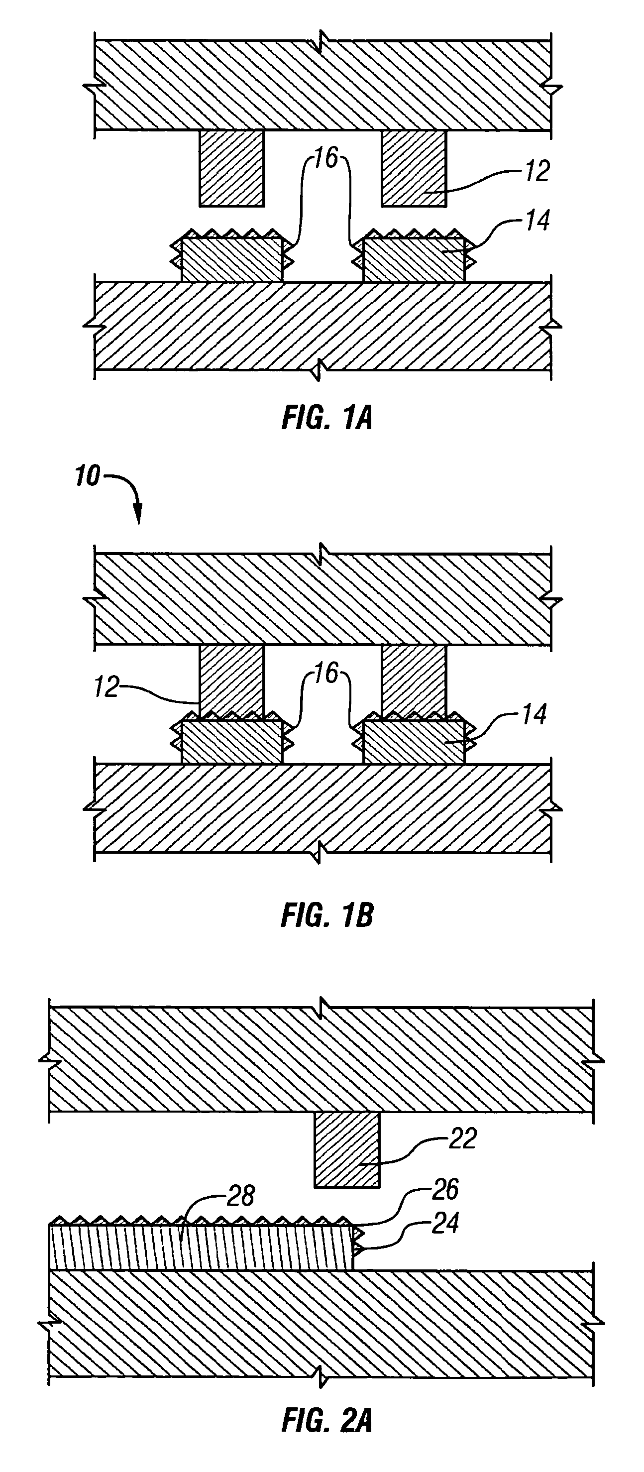
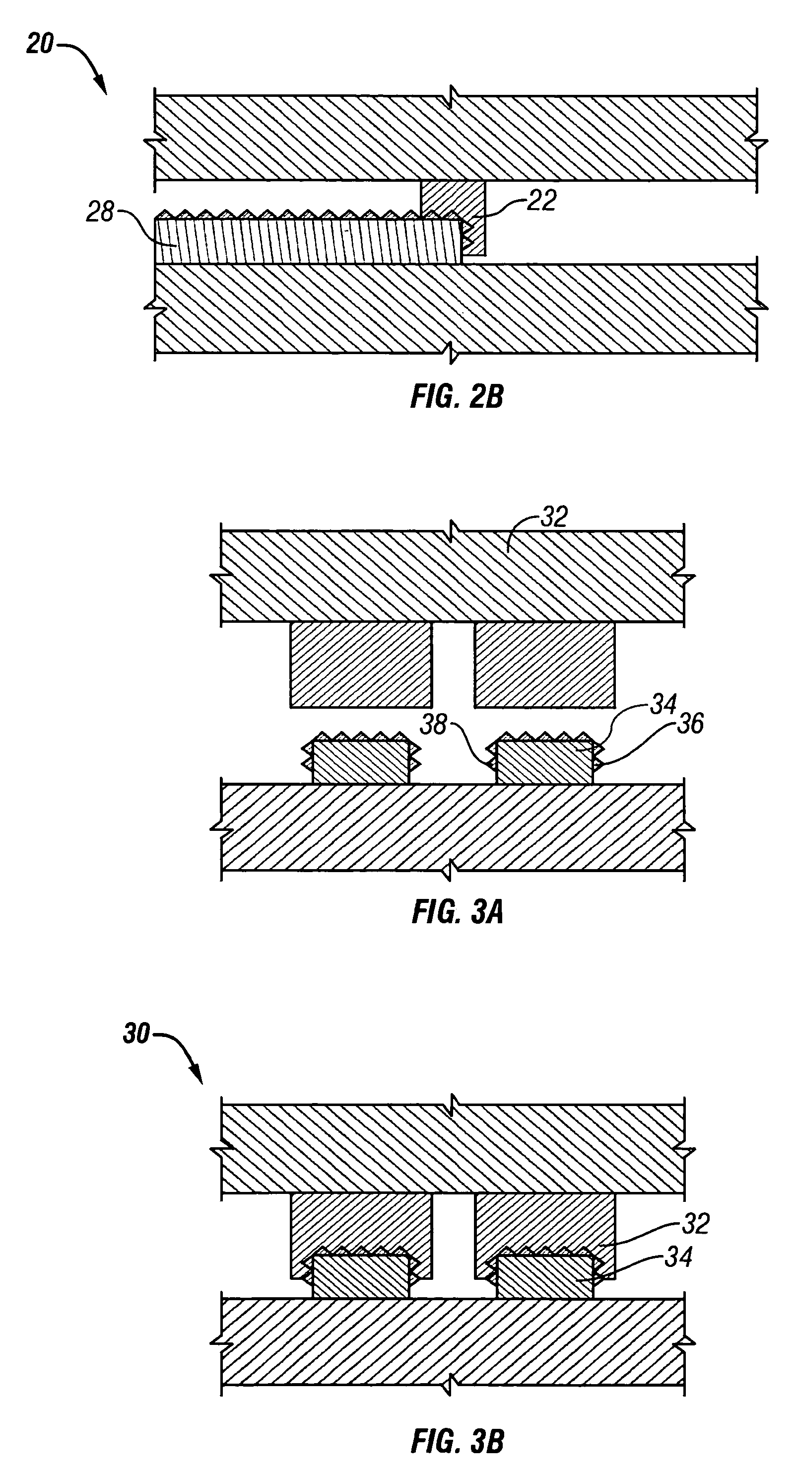
[0016]A second embodiment is schematically shown in FIGS. 2A, 2B. A macroscopic interlocking configuration generally designated 20 is formed by plastic flow of the material of first member 22 around a side wall 24 and edge 26 of a second member or trace 28. Preferably the flow of the material of first member 22 is around the side wall 24 and does not cause material flow into a region between adjacent traces but rather in the normal direction within the same plane. The interlocking configuration 20 provides for an increased area of interlocked surfaces without significantly increasing the bonding force, thereby providing a more robust connection. Further the additional displacement perpendicular to the chip surface provides greater tolerance to poor co-planarity of multiple mating surface. Finally, the interlocking along a plane perpendicular to the chip surface in addition to the usual interlocking parallel to the chip surface provides for protection against relative movement betwee...
third embodiment
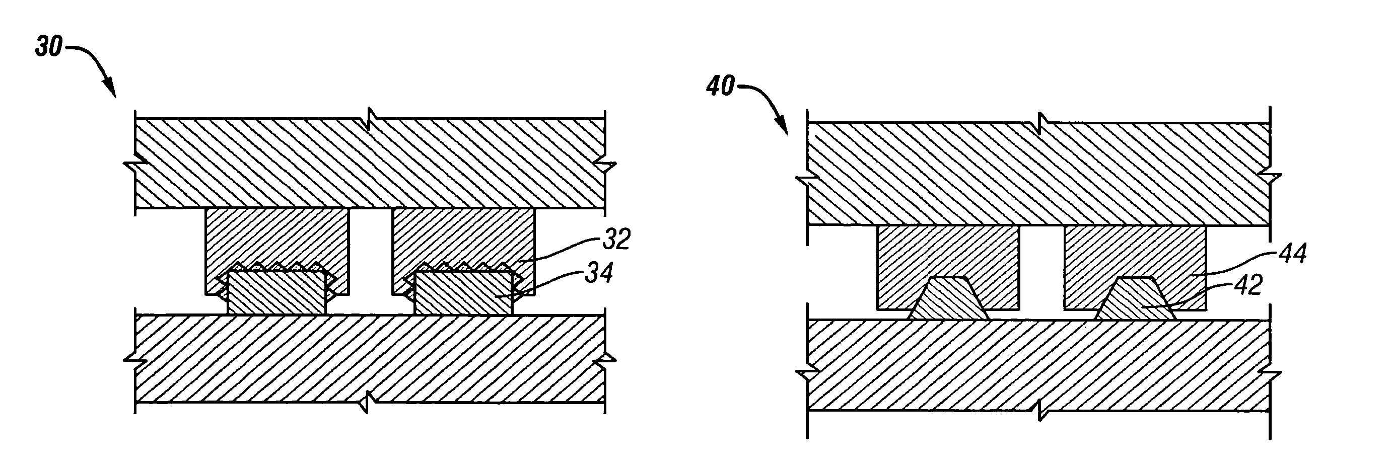
[0017]A third embodiment is shown in FIGS. 3A, 3B and includes an interconnection generally designated 30. The interconnection 30 is formed by plastic flow of the material of a first member 32 around a second member 34. The second member 34 includes a smaller width than that of the first member 32 which allows for plastic flow of the material of first member 32 around both sides 36 and 38 of the second member 34.
fourth embodiment
[0018]A fourth embodiment is shown in FIGS. 4A, 4B and includes an interconnection generally designated 40. The lead geometry of a second element 42 is shown to be wedge shaped to take advantage of what represents the most typical “undercut” lead shape in actual substrates that are fabricated by the subtractive etching method. The interconnection 40 is formed by plastic flow of the material of a first element 44 around the second element 42. The shown geometry removes the restriction of minimum trace width and more specifically the minimum width of a plateau 46 necessary for conventional wire bonding applications. It is contemplated that the interconnection 40 could alternatively be formed by bonding directly on a via pad or through a via hole down to the next lower layer on the substrate.
[0019]In embodiments as described above with reference to FIGS. 2A, 2B, 3A, 3B, 4A, 4B, the macroscopic interlocking configuration allows for formation of the interconnect using a lower force, for ...
PUM
| Property | Measurement | Unit |
|---|---|---|
| Width | aaaaa | aaaaa |
| Elongation | aaaaa | aaaaa |
| Yield strength | aaaaa | aaaaa |
Abstract
Description
Claims
Application Information