
Shallow junction semiconductor and method for the fabrication thereof

a semiconductor and low-passage technology, applied in the field of semiconductor integrated circuit devices, can solve the problems of reducing product yield and reliability, affecting the performance of transistors, and integrated circuits, and achieve the effect of improving the formation of shallow source/drain junctions

Inactive Publication Date: 2006-04-25
ADVANCED MICRO DEVICES INC
View PDF7 Cites 11 Cited by
  • Summary
  • Abstract
  • Description
  • Claims
  • Application Information

AI Technical Summary

Benefits of technology

[0021]The present invention provides a method of forming an integrated circuit. A gate dielectric is formed on a semiconductor substrate, and a gate is formed on the gate dielectric. A super-saturated doped source silicide metallic layer is formed on the semiconductor substrate adjacent the gate and the gate dielectric. The silicide metallic layer incorporates a substantially uniformly distributed dopant therein in a substantially uniform super-saturated concentration. The silicide metallic layer is reacted with the semiconductor substrate therebeneath to form a salicide layer and outdiffuse the dopant from the salicide layer into the semiconductor substrate therebeneath. The outdiffused dopant in the semiconductor substrate is then activated to form a shallow source / drain junction beneath the salicide layer. An interlayer dielectric is then deposited above the semiconductor substrate, and contacts are formed in the interlayer dielectric to the salicide layer. This method significantly improves the formation of very shallow source / drain junctions for integrated circuits.

Problems solved by technology

Integrated circuits are made in and on silicon wafers by extremely complex systems that require the coordination of hundreds or even thousands of precisely controlled processes to produce a finished semiconductor wafer.
As transistors have decreased in size, it has been found that the electrical resistance between the metal contacts and the silicon substrate or the polysilicon has increased to the level where it negatively impacts the performance of the transistors.
With the continuous decrease in device sizes (transistors becoming narrower and thinner and transistor channels becoming shorter), salicidation problems like junction punchthrough, current leakage, and contact resistance continue to reduce product yields and reliability.
In general, salicidation results in high junction leakage due to metal penetration into the silicon substrate.
The penetration of the metal “spikes” the junction, causing the current leakage.
Residual metal from the salicidation process can also cause leakage.
The residual metal can cause a bridge between adjacent circuit features, like the gate and the S / D regions, causing current leakage.
However, existing shallow S / D junction fabrication technologies, such as ion implantation followed by rapid thermal annealing, have not succeeded in solving all the problems related to fabricating increasingly shallow S / D junctions, and to connecting metal contacts to them.
Solutions to these problems have been long sought but prior developments have not taught or suggested any solutions and, thus, solutions to these problems have long eluded those skilled in the art.

Method used


Image

  • Shallow junction semiconductor and method for the fabrication thereof
  • Shallow junction semiconductor and method for the fabrication thereof
  • Shallow junction semiconductor and method for the fabrication thereof

Examples


Embodiment Construction

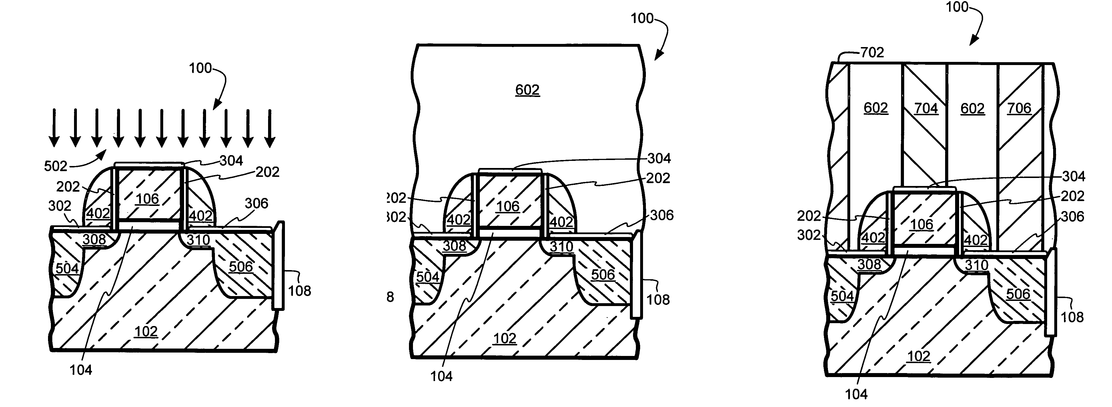
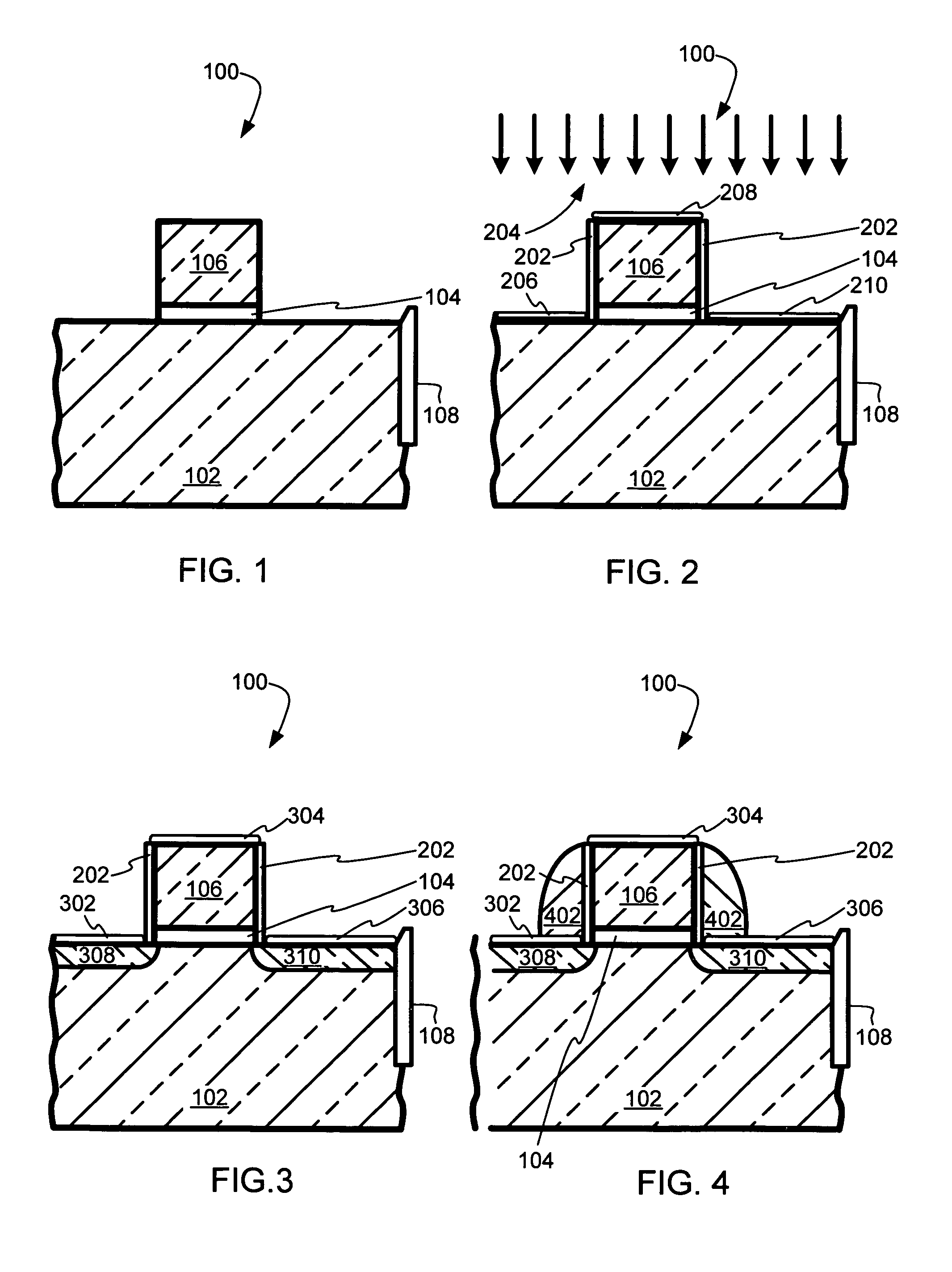
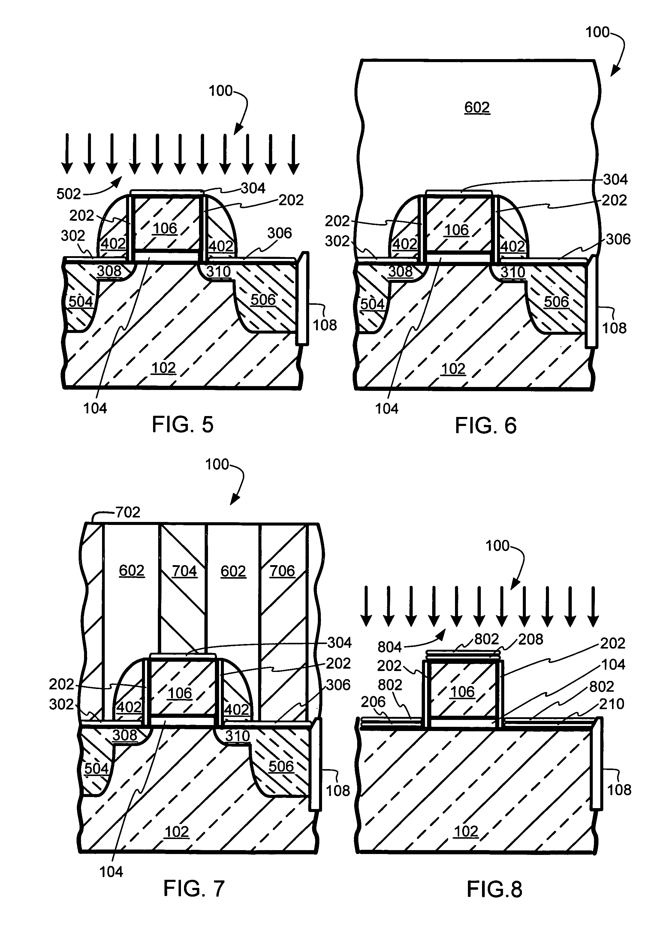
[0035]In the following description, numerous specific details are given to provide a thorough understanding of the invention. However, it will be apparent to one skilled in the art that the invention may be practiced without these specific details. In order to avoid obscuring the present invention, some well-known configurations and process steps are not disclosed in detail. In addition, the drawings showing embodiments of the device are semi-diagrammatic and not to scale and, particularly, some of the dimensions are for the clarity of presentation and may be exaggerated in the drawing FIGS. The same numbers will be used in all the drawing FIGS. to relate to the same elements.

[0036]The term “horizontal” as used herein is defined as a plane parallel to a substrate or wafer. The term “vertical” refers to a direction perpendicular to the horizontal as just defined. Terms, such as “on”, “above”, “below”, “bottom”, “top”, “side” (as in “sidewall”), “higher”, “lower”, “over”, and “under”,...


PUM


Abstract

A method of forming an integrated circuit with a semiconductor substrate is provided. A gate dielectric is formed on the semiconductor substrate, and a gate is formed on the gate dielectric. A super-saturated doped source silicide metallic layer is formed on the semiconductor substrate adjacent the gate and the gate dielectric. The silicide metallic layer incorporates a substantially uniformly distributed dopant therein in a substantially uniform super-saturated concentration. The silicide metallic layer is reacted with the semiconductor substrate therebeneath to form a salicide layer and outdiffuse the dopant from the salicide layer into the semiconductor substrate therebeneath. The outdiffused dopant in the semiconductor substrate is then activated to form a shallow source / drain junction beneath the salicide layer. An interlayer dielectric is then deposited above the semiconductor substrate, and contacts are formed in the interlayer dielectric to the salicide layer.

Description

BACKGROUND[0001]1. Technical Field[0002]The present invention relates generally to semiconductor technology, and more specifically to shallow junction formation in semiconductor integrated circuit devices.[0003]2. Background Art[0004]At the present time, electronic products are used in almost every aspect of life, and the heart of these electronic products is the integrated circuit. Integrated circuits are used in everything from airplanes and televisions to wristwatches.[0005]Integrated circuits are made in and on silicon wafers by extremely complex systems that require the coordination of hundreds or even thousands of precisely controlled processes to produce a finished semiconductor wafer. Each finished semiconductor wafer has hundreds to tens of thousands of integrated circuits, each wafer worth hundreds or thousands of dollars.[0006]Integrated circuits are made up of hundreds to millions of individual components. One common component is the semiconductor transistor. The most co...

Claims


Application Information

Patent Timeline
Patent Type & Authority Patents(United States)
IPC IPC(8): H01L21/22H01L21/336H01L21/44H01L21/8234
CPCH01L21/26506H01L21/28518H01L29/6659H01L29/665H01L29/6656H01L21/823814
Inventor PELELLA, MARIO M.EN, WILLIAM GEORGEPATON, ERICMASZARA, WITOLD P.
Owner ADVANCED MICRO DEVICES INC
Features
  • Generate Ideas
  • Intellectual Property
  • Life Sciences
  • Materials
  • Tech Scout
  • Unparalleled Data Quality
  • Higher Quality Content
  • 60% Fewer Hallucinations
Learn More