Method for fabricating a silicon carbide interconnect for semiconductor components

a technology of silicon carbide and interconnects, which is applied in the direction of instruments, basic electric elements, solid-state devices, etc., can solve the problems of insufficient electrical conductivity of interconnects, inability to resist deformation, and conductive materials used in interconnects that do not possess sufficient strength to resist deformation, so as to improve the electrical conductivity of interconnect contacts

Inactive Publication Date: 2006-04-25
MICRON TECH INC
View PDF71 Cites 3 Cited by
  • Summary
  • Abstract
  • Description
  • Claims
  • Application Information

AI Technical Summary

Benefits of technology

[0011]As silicon carbide has a mechanical hardness similar to diamond, the silicon carbide layers provide a wear-resistant surface for the interconnect contacts. The wear resistant surface makes the interconnect particularly suitable to testing applications wherein the interconnect contacts are used to perform multiple test procedures on many different components. The silicon carbide layer also has a relatively high strength and a high maximum working temperature, such that the interconnect contacts can resist deformation at temperature.
[0012]In addition, as silicon carbide has a high thermal conductivity, the silicon carbide layers provide efficient heat transfer from the component contacts to the interconnect contacts, and better temperature control at the interface of the interconnect contacts with the component contacts. Further, the silicon carbide layers can be configured to substantially cover the area on the substrate between the interconnect contacts to provide a large surface area for dissipating heat generated by the component.
[0020]The silicon carbide conductive layers can be deposited on the interconnect contacts by chemical vapor deposition through a mask, or by conformal deposition of a layer of silicon carbide on the substrate followed by etching. Also, the silicon carbide conductive layers can be doped during deposition, or implanted following deposition. Alternately, the “as deposited” silicon carbide conductive layers can be subjected to localized heat with a laser beam to improve the electrical conductivity of the interconnect contacts. A silicon carbide layer can also be deposited, or patterned, to form the conductors and the terminal contacts as well as a large area heat transfer surface on the interconnect.

Problems solved by technology

One aspect of silicon is that it is a semiconductor material, and does not have sufficient electrical conductivity to permit signal transmission.
Some of the conductive materials used in interconnects do not possess sufficient strength to resist deformation during fabrication or use of electronic assemblies.
For example, in test systems, some conductive materials, such as metals, are prone to wear and oxidation with continued usage.
Also, some conductive materials, such as metal silicides, do not possess a thermal conductivity which permits efficient heat dissipation from the component.

Method used


Image

  • Method for fabricating a silicon carbide interconnect for semiconductor components
  • Method for fabricating a silicon carbide interconnect for semiconductor components
  • Method for fabricating a silicon carbide interconnect for semiconductor components

Examples


Embodiment Construction

[0038]As used herein, the term “semiconductor component” refers to an electrical element or assembly that contains a semiconductor die. Exemplary semiconductor components include bare semiconductor dice, chip scale packages, conventional semiconductor packages, wafers containing dice or chip scale packages, panels containing chip scale packages, boards containing semiconductor dice, and electronic assemblies, such as field emission displays, containing semiconductor dice.

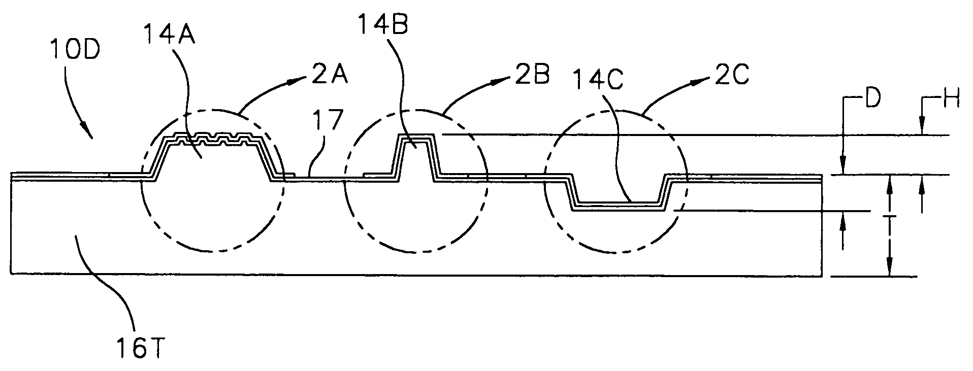
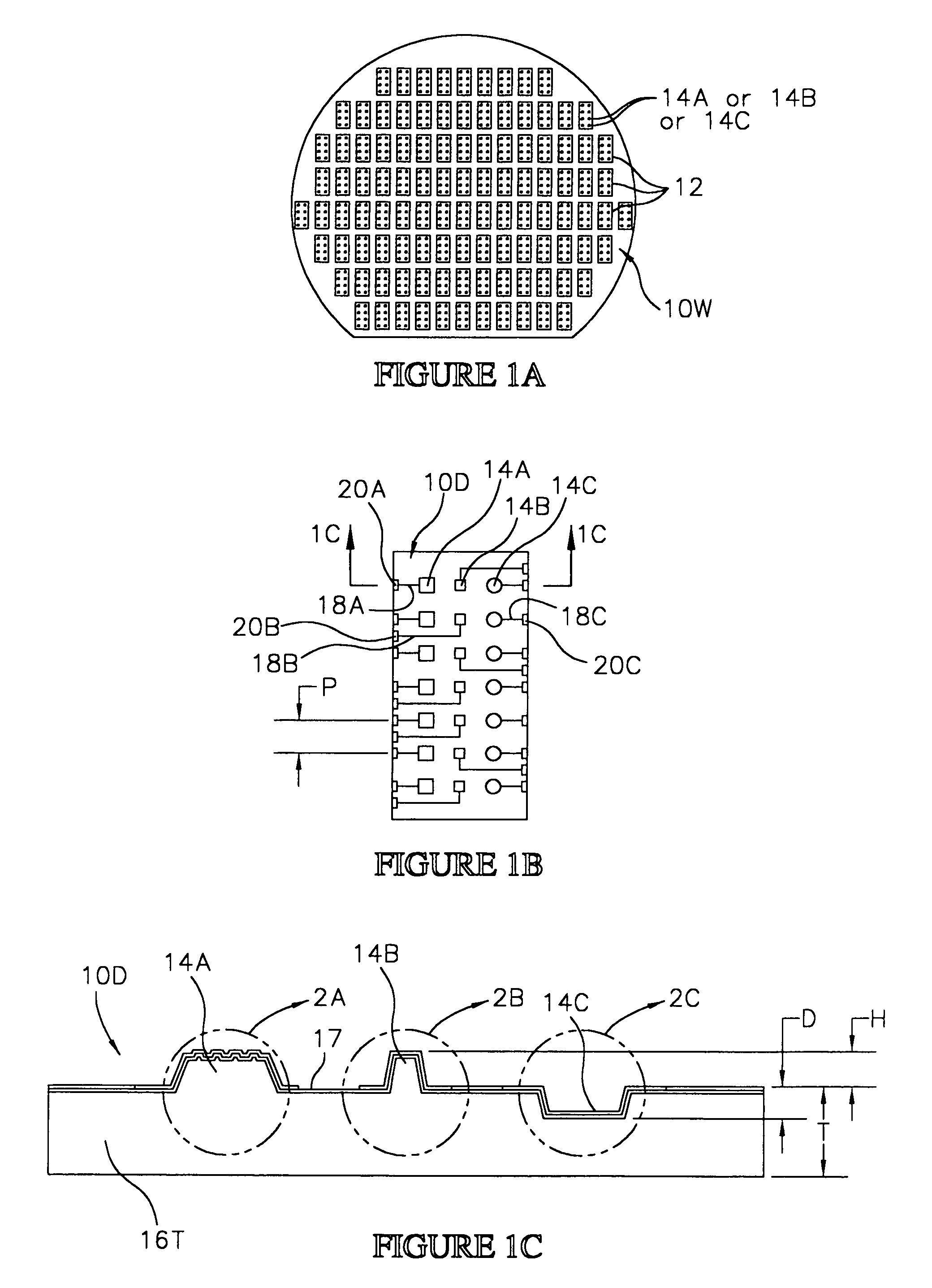
[0039]In FIG. 1A, a wafer level interconnect 10W is illustrated. The interconnect 10W is adapted to electrically engage wafer sized components such as semiconductor wafers. In the illustrative embodiment, the interconnect 10W has the peripheral shape of a semiconductor wafer. However, depending on the components being electrically engaged, other peripheral shapes are possible. In addition, the interconnect 10W includes a plurality of contact sites 12 corresponding to the location of the dice on the wafer. Again, the...


PUM

PropertyMeasurementUnit
heightaaaaaaaaaa
depthaaaaaaaaaa
penetration depthaaaaaaaaaa

Abstract

An interconnect for semiconductor components includes a substrate, and interconnect contacts on the substrate for electrically engaging component contacts on the components. The interconnect contacts include silicon carbide conductive layers, and conductors in electrical communication with the silicon carbide conductive layers. The silicon carbide conductive layers provides a wear resistant surface, and improved heat transfer between the component contacts and the interconnect contacts. The silicon carbide conductive layers can comprise doped silicon carbide, or alternately thermally oxidized silicon carbide. The interconnect can be configured for use with a testing apparatus for testing discrete components such as dice or chip scale packages, or alternately for use with a testing apparatus for testing wafer sized components, such as wafers, panels and boards. In addition, the interconnect can be configured for constructing semiconductor packages and electronic assemblies such as multi chip modules.

Description

CROSS REFERENCE TO RELATED APPLICATIONS[0001]This application is a division of patent application Ser. No. 09 / 480,027, now U.S. Pat. No. 6,563,215, filed on Jan. 10, 2000.FIELD OF THE INVENTION[0002]This invention relates generally to semiconductor manufacture and specifically to an improved interconnect for electrically engaging semiconductor components such as dice, packages, wafers, panels, boards, and electronic assemblies containing dice or packages.BACKGROUND OF THE INVENTION[0003]Different types of semiconductor components include terminal contacts which provide electrical connection points for applying electronic signals to the integrated circuits contained on the components. For example, bare dice and semiconductor wafers typically include bond pads which function as terminal contacts. Chip scale packages typically include solder balls, which function as terminal contacts. Electronic assemblies, such as circuit boards and field emission displays, can include pads, solder ba...

Claims


Application Information

Patent Timeline
Patent Type & Authority Patents(United States)
IPC IPC(8): H01L21/44G01R1/067G01R1/073H01L23/13H01L23/498
CPCG01R3/00H01L23/13H01L23/147H01L23/498G01R1/06755H01L23/49872H01L23/49877H01L23/49838G01R1/06711G01R1/07314H01L2924/09701H01L2924/0002H01L2924/00
Inventor AKRAM, SALMANWOOD, ALAN G.
Owner MICRON TECH INC
Why Eureka
Try Eureka