Strip conductor arrangement and method for producing a strip conductor arrangement

a technology of strip conductors and interconnects, which is applied in the direction of electrical equipment, semiconductor devices, semiconductor/solid-state device details, etc., can solve the problems of high power loss, high signal propagation times, crosstalk, etc., and achieve the reduction of overall capacitance within the integrated circuit, reduce undesirable leakage fields, and reduce the capacitance between these interconnects

Inactive Publication Date: 2006-04-25
INFINEON TECH AG
View PDF8 Cites 23 Cited by
  • Summary
  • Abstract
  • Description
  • Claims
  • Application Information

AI Technical Summary

Benefits of technology

[0011]One advantage of the invention is that, on account of the very large cavity as insulating layer between adjacent interconnects, the effective relative dielectric constant ∈r of the insulating layer between the adjacent interconnects deviates only slightly from one, and therefore the capacitance between these interconnects is reduced. The interconnect arrangement allows a considerable reduction in the overall capacitance within an integrated circuit.
[0012]A further advantage of the interconnect arrangement is that the cavity considerably reduces undesirable leakage fields between the interconnects, which are produced by the interconnects above and / or below the actual interconnect layer in the interconnect arrangement. Therefore, the effective relative dielectric constant ∈r, which is influenced both by the relative dielectric constant of the cavity and by that of the surrounding material, is approximately two. In this case, the value of the effective relative dielectric constant ∈r is dependent on the geometry of the entire interconnect arrangement.
[0013]Furthermore, there is the advantage of a high stability during the fabrication of the interconnect arrangement, since, during the planarization of the interconnects in a chemical mechanical polishing (CMP) operation during production of the interconnects, the latter are still embedded in the solid substrate. The cavity is only introduced into the substrate after the interconnects have been produced, and therefore the mechanical stability of the substrate is only reduced at that time.
[0014]Moreover, coupling capacitances between the interconnects are avoided on account of etching and / or CMP stop layers. This is because these stop layers, during production of the cavity, preferably by means of etching, are interrupted in such a manner that adjacent interconnects are not in physical contact as a result of a stop layer of this type.
[0015]After completion of the interconnect arrangement, the cavity preferably contains air, a vacuum or an electrically insulating gas in order to improve the resistance to electrical spark-overs, for example sulphur hexafluoride (SF6).
[0017]The cavity preferably extends partially into the covering layer situated on the substrate. This contributes to an additional reduction in the effective relative dielectric constant ∈r.

Problems solved by technology

As a result, capacitances which are formed between the interconnects rise and lead to high signal propagation times, high power losses and crosstalk.

Method used


Image

  • Strip conductor arrangement and method for producing a strip conductor arrangement
  • Strip conductor arrangement and method for producing a strip conductor arrangement
  • Strip conductor arrangement and method for producing a strip conductor arrangement

Examples


Embodiment Construction

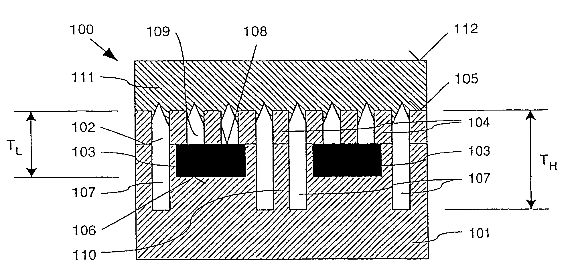
[0061]FIG. 1 shows a cross section perpendicular to the substrate surface 102 through an interconnect arrangement 100 in accordance with a first exemplary embodiment of the invention.

[0062]The interconnect arrangement 100 comprises a substrate 101 with a substrate surface 102. On the substrate surface 102 there is arranged a buffer layer 104 which comprises a buffer-layer surface 105 oriented parallel to the substrate surface 102 above the buffer layer 104. The substrate material selected is a first electrically insulating material, in accordance with this exemplary embodiment solid silicon dioxide (SiO2). The material selected for the buffer layer 104 is a second electrically insulating material, in accordance with this exemplary embodiment once again solid silicon dioxide (SiO2). In the substrate 101 there are a plurality of buried interconnects 103 which are arranged next to one another in such a manner that the respective lower interconnect surface 106, perpendicular to the buff...


PUM


Abstract

An interconnect arrangement comprises a substrate made from a first insulating material with a substrate surface, at least two interconnects which are arranged next to one another in the substrate, a buffer layer made from a second insulating material above the substrate and comprising a buffer-layer surface, which is parallel to the substrate surface, at least one cavity, which is arranged between the interconnects and, with respect to the buffer-layer surface, extends deeper into the substrate than the interconnects, and a covering layer made from a third insulating material, which is arranged above the buffer layer and completely closes off the cavity with respect to the buffer-layer surface.

Description

CROSS-REFERENCE TO RELATED APPLICATIONS[0001]This application is a U.S. National-Stage entry under 35 U.S.C. § 371 based on International Application No. PCT / DE02 / 02946, filed 09 Aug. 2002, which was published under PCT Article 21(2); this application also claims priority under 35 U.S.C. § 119 to German Application No. DE 101 40 754.8, filed Aug. 20, 2001.BACKGROUND OF THE INVENTION[0002]The invention relates to an interconnect arrangement and to a method for fabricating an interconnect arrangement.[0003]Integrated circuit arrangements are being produced with an ever greater packing density. The result of this is that interconnects in metallization layers are at an ever decreasing spacing from one another. As a result, capacitances which are formed between the interconnects rise and lead to high signal propagation times, high power losses and crosstalk. Hitherto, SiO2, the relative dielectric constant of which is εr=3.9, has primarily been used as the dielectric for providing insula...

Claims


Application Information

Patent Timeline
Patent Type & Authority Patents(United States)
IPC IPC(8): H01L21/4763H01L21/768H01L23/522
CPCH01L23/5222H01L21/7682H01L2924/0002H01L2924/00
Inventor SCHINDLER, GUNTHERPAMLER, WERNERGABRIC, ZVONIMIR
Owner INFINEON TECH AG
Why Eureka
Try Eureka