ONO fabrication process for increasing oxygen content at bottom oxide-substrate interface in flash memory devices

a fabrication process and flash memory technology, applied in the field of semiconductor device preparation, can solve the problem of limiting the scaling down of the total physical thickness of the ono layer, and achieve the effects of increasing the oxygen content, reducing the thermal budget, and distinct process and economic advantages

Inactive Publication Date: 2006-04-25
LONGITUDE FLASH MEMORY SOLUTIONS LTD
View PDF15 Cites 59 Cited by
  • Summary
  • Abstract
  • Description
  • Claims
  • Application Information

AI Technical Summary

Benefits of technology

[0011]Thus, the present invention, by providing an increased oxygen content in the bottom oxide layer of the ONO structure in a flash memory device, a bottom oxide layer may be fabricated without creation of interface states resulting from oxygen vacancies, E′ centers and dangling bonds, which could provide charge leakage paths from the charge-storage layer. The present invention can be carried out in a cluster tool. The present invention provides advantages such as (1) formation of a bottom oxide / substrate interface with a higher oxygen content; (2) allowing selection of any of a number of different methods for increasing the oxygen content; (3) a lower thermal budget; and (4) formation of a sharper bottom oxide / substrate interface, resulting in fewer interface states that could provide charge leakage paths. Thus, the present invention provides an advance in ONO fabrication technology, and insures proper charge isolation in ONO structures used in MIRRORBIT™ two-bit EEPROM devices, while at the same time providing distinct process and economic advantages. Although described in terms of, and particularly applicable to, MIRRORBIT™ two-bit EEPROM devices, the present invention is broadly applicable to fabrication of any semiconductor device that includes an ONO structure.

Problems solved by technology

However, as the ONO layer is made physically thinner, leakage currents through the ONO layer may increase, which limits the scaling down of the total physical thickness of the ONO layer.
While the recent advances in EEPROM technology have enabled memory designers to double the memory capacity of EEPROM arrays using two-bit data storage, numerous challenges exist in the fabrication of material layers within these devices.

Method used


Image

  • ONO fabrication process for increasing oxygen content at bottom oxide-substrate interface in flash memory devices
  • ONO fabrication process for increasing oxygen content at bottom oxide-substrate interface in flash memory devices
  • ONO fabrication process for increasing oxygen content at bottom oxide-substrate interface in flash memory devices

Examples


first embodiment

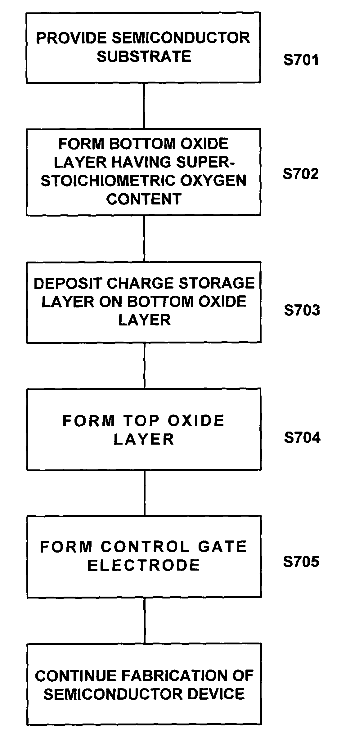
[0025]The present invention broadly includes two embodiments. In the present invention, shown schematically in FIG. 7, a bottom oxide layer 28 is formed by a conventional process to include a first oxygen content, and is thereafter treated to increase the oxygen content from the first oxygen content to a second oxygen content. In one embodiment, the bottom oxide layer having the second oxygen content exhibits a reduced charge leakage relative to the bottom oxide layer having the first oxygen content.

second embodiment

[0026]In the present invention, shown schematically in FIG. 8, a bottom oxide layer 28 is formed by novel methods which provide the bottom oxide layer 28 with a super-stoichiometric oxygen content. In one embodiment, the super-stoichiometric oxygen content provides an increased oxygen content relative to the oxygen content in a conventional bottom oxide. In one embodiment, the bottom oxide layer having the super-stoichiometric oxygen content exhibits a reduced charge leakage relative to a conventional bottom oxide layer.

[0027]The first step of both embodiments is the same. In the first step of the present invention, shown schematically in FIG. 7 as Step 701 and in FIG. 8 as Step 801, a semiconductor substrate is provided. The semiconductor substrate may be any appropriately selected semiconductor substrate known in the art. In one embodiment, the semiconductor substrate is a bulk silicon substrate. In one embodiment, the semiconductor substrate is a silicon-on-insulator semiconducto...


PUM

PropertyMeasurementUnit
temperatureaaaaaaaaaa
temperaturesaaaaaaaaaa
temperatureaaaaaaaaaa

Abstract

Process for reducing charge leakage in a SONOS flash memory device, including in one embodiment, forming a bottom oxide layer of an ONO structure on the semiconductor substrate to form an oxide/silicon interface having a first oxygen content adjacent the oxide/silicon interface; treating the bottom oxide layer to increase the first oxygen content to a second oxygen content adjacent the oxide/silicon interface; and depositing a nitride charge-storage layer on the bottom oxide layer. In another embodiment, process for reducing charge leakage in a SONOS flash memory device, including forming a bottom oxide layer of an ONO structure on a surface of the semiconductor substrate having an oxide/silicon interface with a super-stoichiometric oxygen content adjacent the oxide/silicon interface; and depositing a nitride charge-storage layer on the bottom oxide layer.

Description

TECHNICAL FIELD[0001]The present invention relates to a process for preparation of a semiconductor device including forming an ONO structure. The bottom oxide-substrate interface is provided with increased oxygen content.BACKGROUND ART[0002]Non-volatile memory devices are currently in widespread use in electronic components that require the retention of information when electrical power is terminated. Non-volatile memory devices include read-only-memory (ROM), programmable-read-only memory (PROM), erasable-programmable-read-only memory (EPROM), and electrically-erasable-programmable-read-only-memory (EEPROM) devices. EEPROM devices differ from other non-volatile memory devices in that they can be electrically programmed and erased. Flash EEPROM devices are similar to EEPROM devices in that memory cells can be programmed and erased electrically. However, flash EEPROM devices enable the erasing of all memory cells in the device using a single electrical current pulse.[0003]Product dev...

Claims


Application Information

Patent Timeline
Patent Type & Authority Patents(United States)
IPC IPC(8): H01L21/31
CPCH01L21/28273H01L21/3144H01L29/66825H01L29/792H01L29/513Y10S438/954H01L29/40114H01L21/022
Inventor SHIRAIWA, HIDEHIKOKAMAL, TAZRIENRAMSBEY, MARKKANG, INKUKPARK, JAEYONGSUGINO, RINJIYANG, JEAN Y.CHEUNG, FRED T KHALLIYAL, ARVINDJAFARPOUR, AMIR H.
Owner LONGITUDE FLASH MEMORY SOLUTIONS LTD
Why Eureka
Try Eureka