Processing systems and methods that reduce even-order harmonic energy
a processing system and harmonic energy technology, applied in the field ofdifferential processing systems, can solve the problems of excessive signal harmonics and relentless increase in linearity demands of these processing systems
- Summary
- Abstract
- Description
- Claims
- Application Information
AI Technical Summary
Problems solved by technology
Method used
Image
Examples
embodiment 60
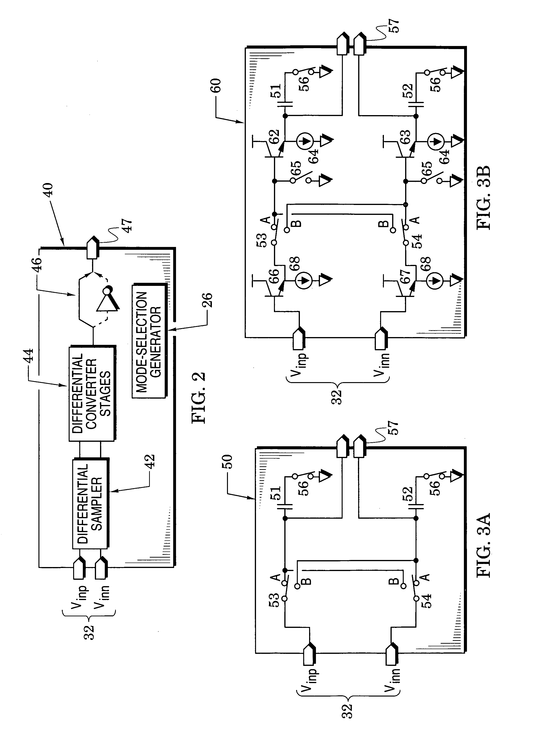
[0026]FIG. 3B illustrates another differential sampler embodiment 60 that is similar to the sampler 50 with like elements indicated by like reference numbers. The sampler 60 inserts first and second buffer transistors 62 and 63 between the first and second switches and the first and second capacitors (each buffer has a corresponding current source 64). The buffers are arranged as emitter followers that can be enabled to capture signal samples on the first and second capacitors and then disabled (e.g., by grounding bases through shorting switches 65) as these samples are being processed through the converter stages (44 in FIG. 2).
[0027]The upstream isolation provided by the downstream current gain (upstream current loss) of the buffers 62 and 63 has been found to enhance the accuracy of the signal samples. This isolation is further enhanced by inserting third and fourth buffer transistors 66 and 67 ahead of the first and second switches 53 and 54 (each buffer has a corresponding curr...
embodiment 70
[0028]FIG. 3C illustrates a differential sampler embodiment 70 that is similar to the sampler 60 of FIG. 3B with like elements indicated by like reference numbers. The sampler 70 realizes the switch 53 of FIG. 3B with a pair of switch transistors 53A and 53B and realizes the switch 54 with a pair of switch transistors 54A and 54B. Sources of the transistors 53A and 53B are coupled to their respective upstream buffer 66 with their drains coupled respectively to downstream buffers 62 and 63. Sources of the transistors 54A and 54B are coupled to their respective upstream buffer 66 with their drains coupled respectively to downstream buffers 63 and 62.
[0029]A bootstrap system is formed by bootstrap modules 71 that are each coupled between source and gate of a corresponding one of the switch transistors. FIG. 3D illustrates an embodiment of the modules 71 in which the top plate TP of a bootstrap capacitor 72 is coupled to a diode 73 and the bottom plate BP is coupled to a switch 74.
[0030...
embodiment 90
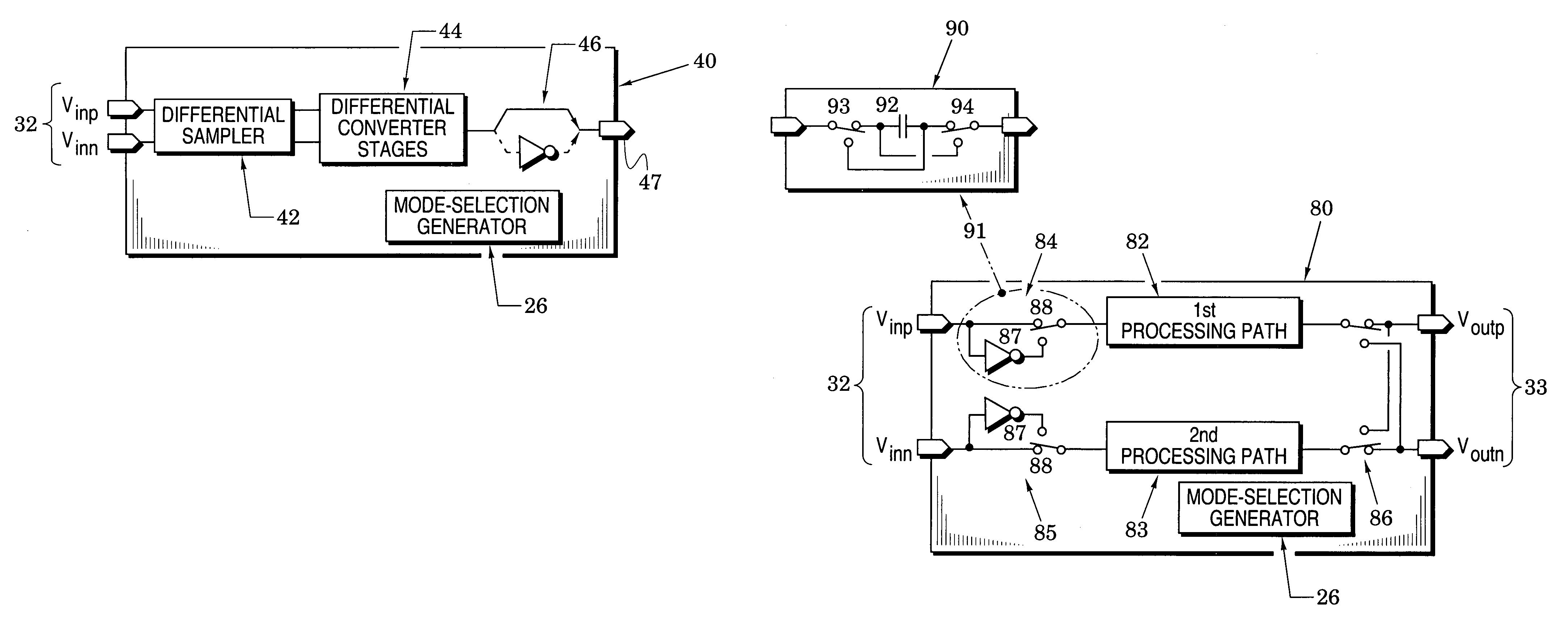
[0040]In FIG. 4, the inverter networks 84 and 85 are realized with inverters 87 which are selected in the second processing mode by activating switches 88. In a sampled-data system, these inverter networks can be replaced by another inverter embodiment 90 as indicated by a replacement arrow 91. The inverter 90 is a reversible-capacitor network that presents a capacitor 92 in a first arrangement in the first processing mode and in a reversed arrangement in the second processing mode to thereby invert the input signal in the second processing mode. The reversible-capacitor network positions the capacitor 92 between first and second reversing switches 93 and 94 which are in the position shown in the first processing mode and in a second position in the second processing mode.
PUM
 Abstract
Description
Claims
Application Information


