

Backflush chamber clean
a technology of backflush and chamber cleaning, which is applied in the direction of cleaning hollow objects, liquid cleaning, coatings, etc., can solve the problems of reducing the efficiency of the cleaning process, so as to achieve the effect of enhancing the concentration of reactive ionic species availabl
- Summary
- Abstract
- Description
- Claims
- Application Information
AI Technical Summary
Benefits of technology
Problems solved by technology
Method used
Image

Examples
Embodiment Construction
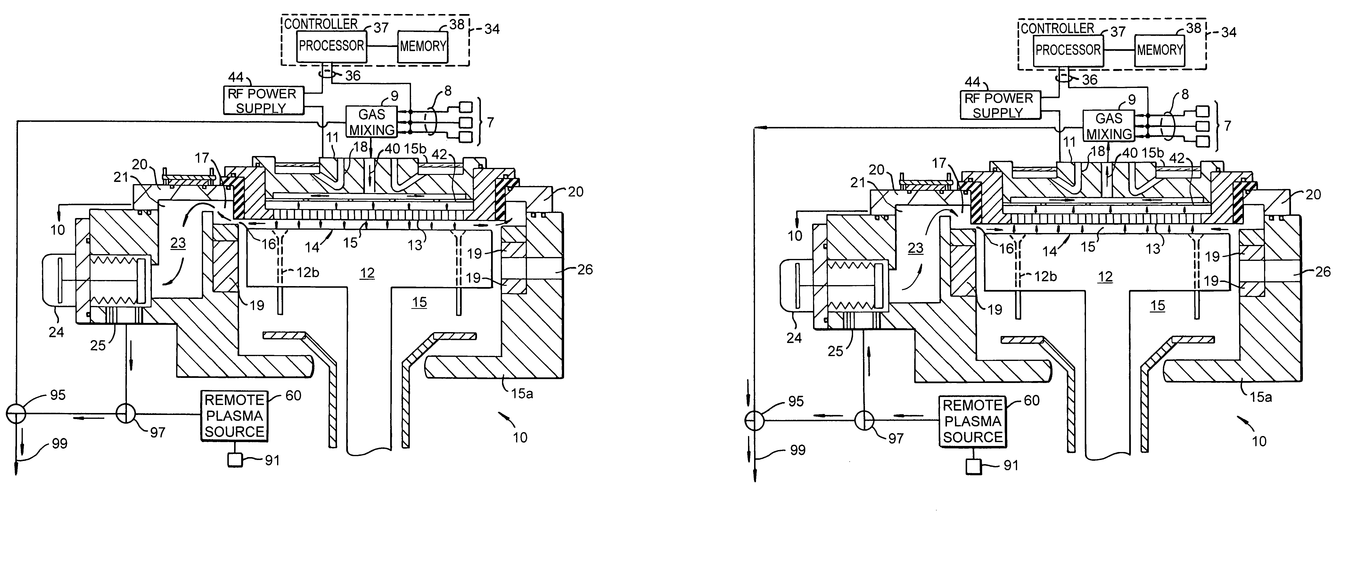
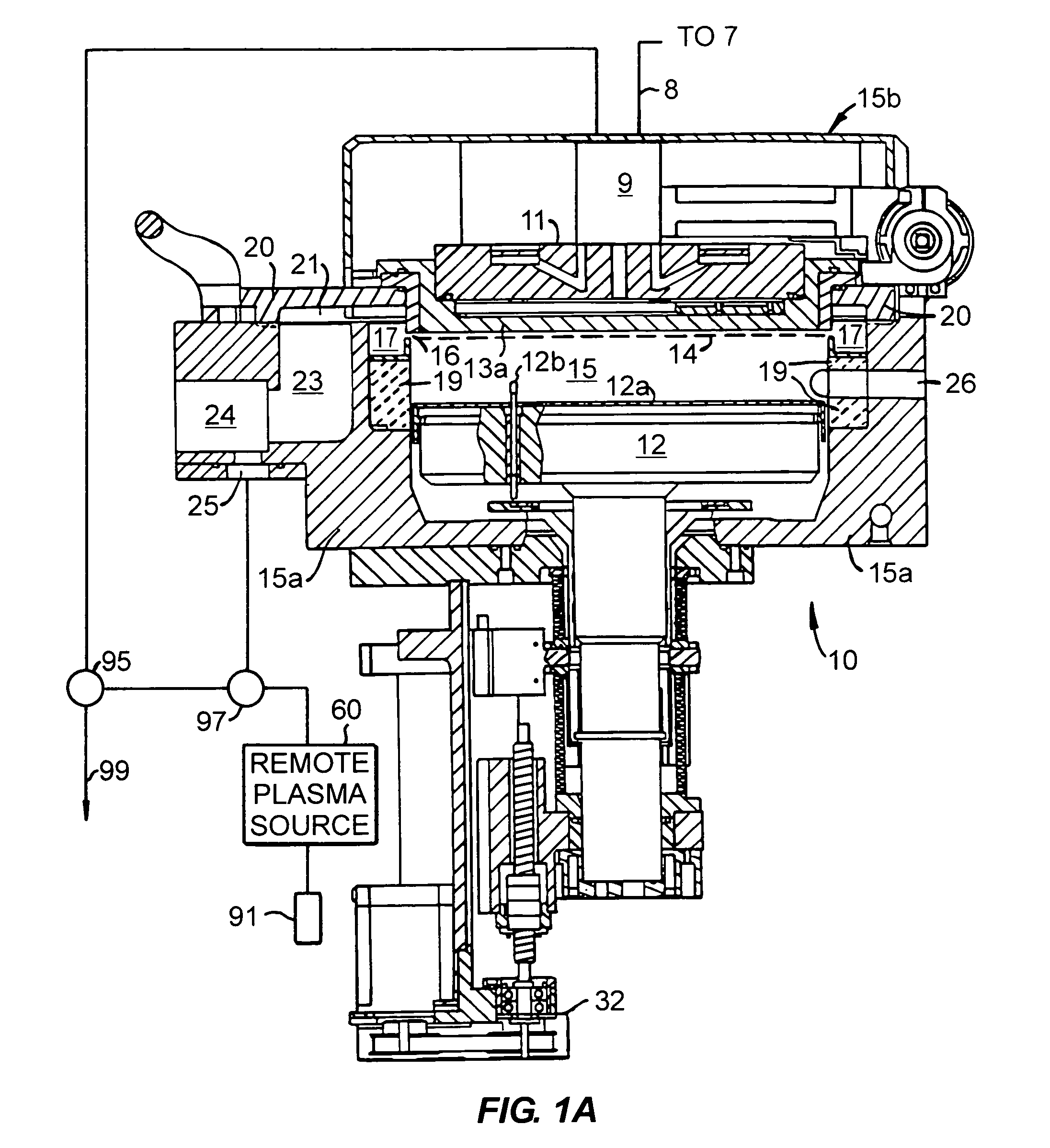
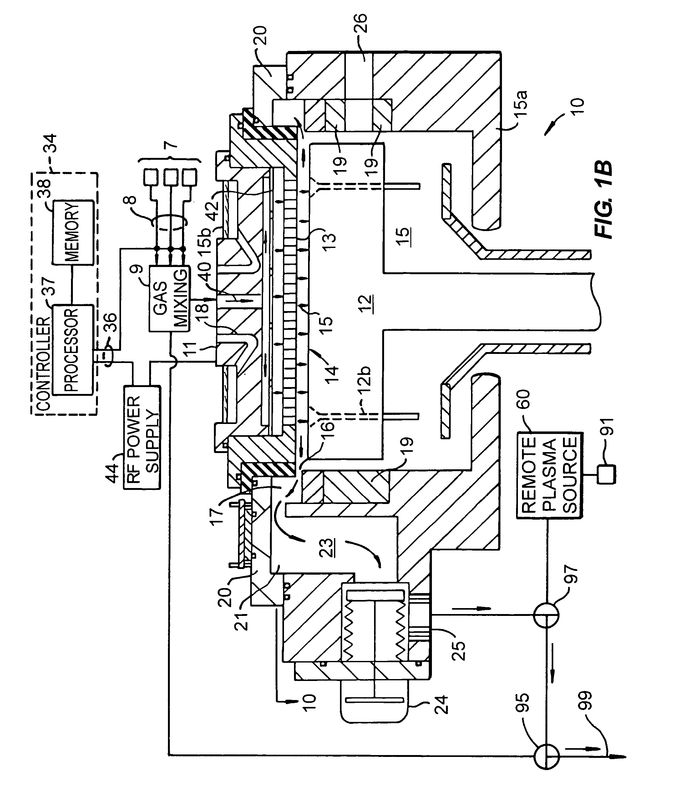
[0023]A processing chamber is effectively cleaned by a remote plasma flowed through the chamber in roughly the opposite direction than is utilized during semiconductor processing. Specifically, the remotely generated plasma may be introduced through a processing gas exhaust port, and then exhausted from the chamber by traveling through the gas distribution shower head to the foreline. In accordance with one embodiment of the present invention, this reverse flow of remote cleaning plasma is maintained throughout the duration of the chamber cleaning step. In accordance with an alternative embodiment of the present invention, the direction of flow of the remote cleaning plasma through the chamber is alternated during the cleaning step between the reverse flow and a conventional forward flow.
[0024]One suitable substrate processing system in which the method of the present invention can be carried out is shown in FIGS. 1A–B, which are vertical, cross-sectional views of a CVD system 10, h...
PUM
| Property | Measurement | Unit |
|---|---|---|
| RF frequency | aaaaa | aaaaa |
| pressure | aaaaa | aaaaa |
| pressure | aaaaa | aaaaa |
Abstract
Description
Claims
Application Information