Electric field induced spin-polarized current

a technology of electric current and electric field, which is applied in the direction of basic electric elements, electrical apparatus, semiconductor devices, etc., can solve the problems of inability to achieve effective spin injection using only nonmagnetic semiconductors, no efficient method of spin generation and injection and inability to achieve the effect of generating and injecting spin in semiconductors at room temperatur

Inactive Publication Date: 2006-05-02
THE BOARD OF TRUSTEES OF THE LELAND STANFORD JUNIOR UNIV
View PDF8 Cites 11 Cited by
  • Summary
  • Abstract
  • Description
  • Claims
  • Application Information

AI Technical Summary

Benefits of technology

[0010]According to one embodiment of the present invention, a device for injecting spin-polarized current into a current output terminal includes a semiconductor structure. The semiconductor structure includes a first end and an opposite second end disposed along the direction of a first axis. The semiconductor structure further includes a third end disposed along the direction of a second axis perpendicular to the first axis. A first electrode is formed on the first end of the semiconductor structure and a second electrode is formed on the second end of the semiconductor structure. The first and second electrodes are disposed to receive an applied electric field. A third electrode, being the current output terminal in the present embodiment, is formed on the third end of the semiconductor structure. The third electrode provides the spin-polarized current when an electric field is applied across the first and second electrodes. In accordance with the present invention, the semiconductor structure includes a hole-doped semiconductor structure or an undoped zero-gap semiconductor structure and includes a semiconductor material whose spin orbit coupling energy is greater than room temperature (300 Kelvin) times the Boltzmann constant.
[

Problems solved by technology

While effective spin injection into semiconductors is necessary for such spintronic devices, effective spin injection using only nonmagnetic semiconductors has been an elusive issue.
No efficient methods of spin generation and injection in a semiconductor at room temperature have been reported up to now.
However, using ferromagnetic metals for spin injection is not practical for most semiconductor applications as ferromagnetic formation is not a common or usual semiconductor processing step and is thus more expensive to implement as spec

Method used


Image

  • Electric field induced spin-polarized current
  • Electric field induced spin-polarized current
  • Electric field induced spin-polarized current

Examples


Embodiment Construction

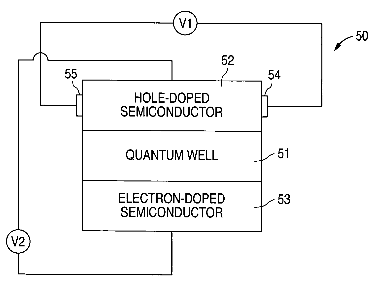
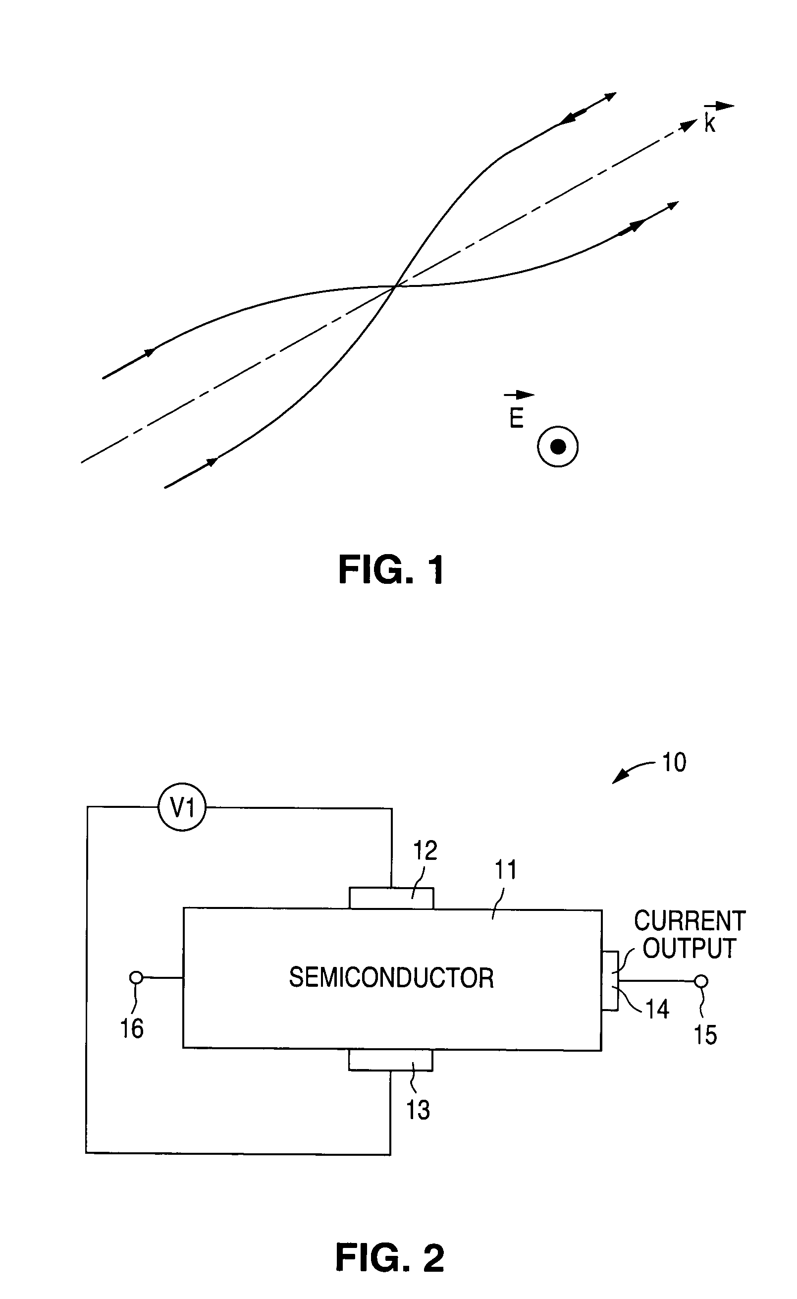
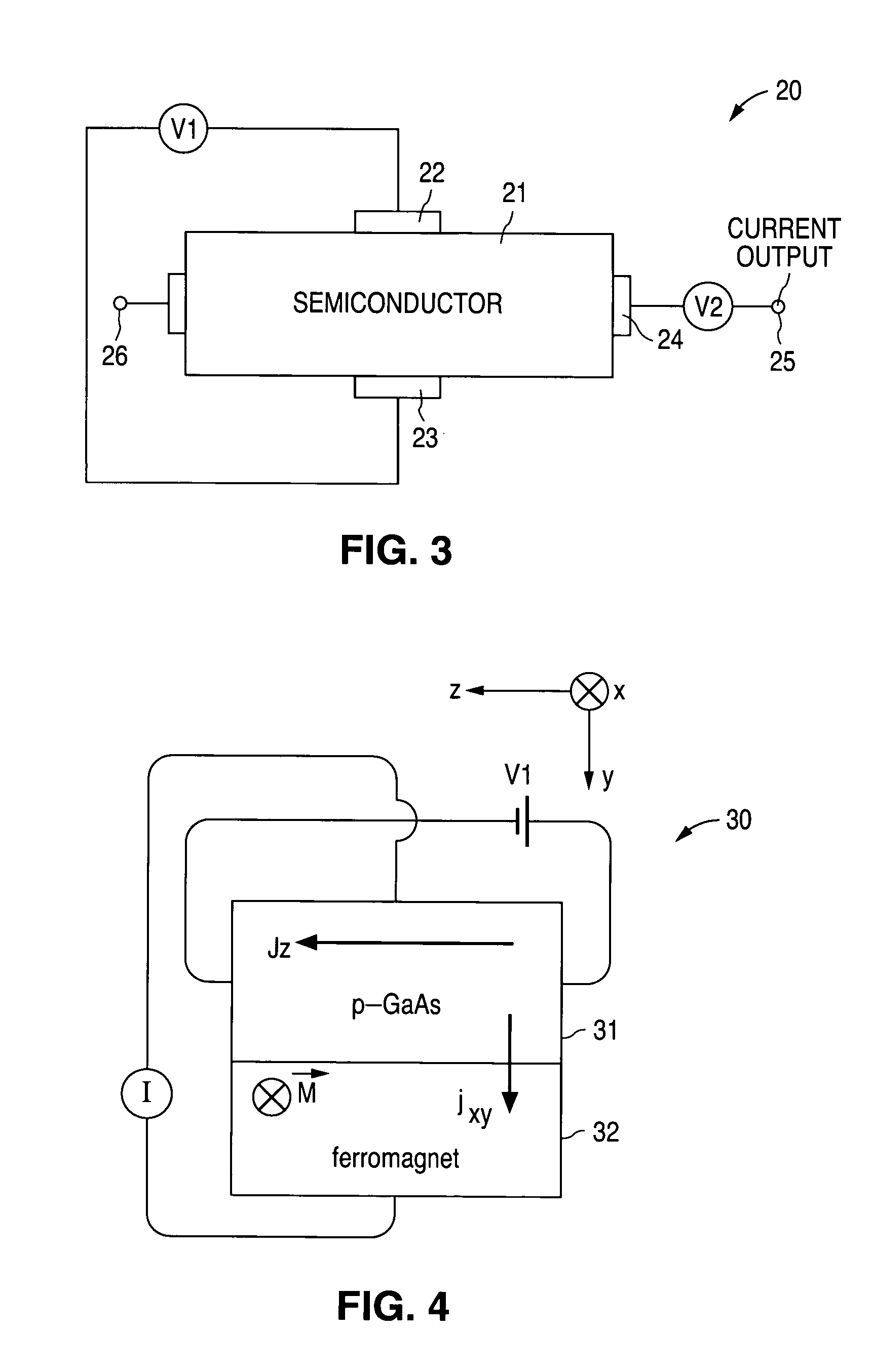
[0022]In accordance with the principles of the present invention, a device and a method for generating a highly spin-polarized electric current utilizes a semiconductor structure and an applied electric field across the semiconductor structure. The semiconductor structure includes a hole-doped semiconductor structure of finite bandgap, a hole-doped semiconductor structure of zero bandgap, or an undoped semiconductor of zero bandgap. In one embodiment, an electric field is applied across a hole-doped semiconductor material having a strong spin orbit coupling energy to generate the spin polarized electric current. The spin current, referred herein as an “electric-field-induced spin current,” can be generated at room temperature and is free from rapid relaxation of spins. Because the spin-polarized electric current is generated in a semiconductor material without the use of metallic ferromagnet or ferromagnetic semiconductor, efficient spin injection in a semiconductor can be realized ...


PUM


Abstract

A device and a method for generating an electric-field-induced spin current are disclosed. A highly spin-polarized electric current is generated using a semiconductor structure and an applied electric field across the semiconductor structure. The semiconductor structure can be a hole-doped semiconductor having finite or zero bandgap or an undoped semiconductor of zero bandgap. In one embodiment, a device for injecting spin-polarized current into a current output terminal includes a semiconductor structure including first and second electrodes, along a first axis, receiving an applied electric field and a third electrode, along a direction perpendicular to the first axis, providing the spin-polarized current. The semiconductor structure includes a semiconductor material whose spin orbit coupling energy is greater than room temperature (300 Kelvin) times the Boltzmann constant. In one embodiment, the semiconductor structure is a hole-doped semiconductor structure, such as a p-type GaAs semiconductor layer.

Description

STATEMENT OF GOVERNMENT SPONSORED RESEARCH[0001]The present invention was made with support from the National Science Foundation under grant no. DMR-9814289 and with support from the US Department of Energy, Office of Basic Energy Sciences, under contract DE-AC03-76SF00515. The US Government has certain rights in the invention.FIELD OF THE INVENTION[0002]The invention relates to a spintronic device and, in particular, to a method of generating spin-polarized electric current in non-magnetic semiconductor materials by applying an electric field.DESCRIPTION OF THE RELATED ART[0003]Spintronics is a field of electronics in which the spin degree of freedom of an electron is utilized for operations of devices. In particular, spintronic devices made using semiconductors have been an important subject of research because of their potential applications in low power devices with integrated logic and storage functions. While effective spin injection into semiconductors is necessary for such s...

Claims


Application Information

Patent Timeline
IPC IPC(8): H01L21/00H01L21/326H01L21/479
CPCH01L29/66984
Inventor MURAKAMI, SHUICHINAGAOSA, NAOTOZHANG, SHOUCHENG
Owner THE BOARD OF TRUSTEES OF THE LELAND STANFORD JUNIOR UNIV
Why Eureka
Try Eureka