Semiconductor device having a non-single crystalline semiconductor layer

a semiconductor layer and semiconductor technology, applied in the direction of semiconductor devices, sustainable manufacturing/processing, climate sustainability, etc., can solve the problems of low photo-sensitivity of this kind of conventional semiconductor photo-electrically-sensitive device, easy to change with the intensity of incident light, and low photo-sensitivity, so as to achieve less variable

Inactive Publication Date: 2006-05-02
SEMICON ENERGY LAB CO LTD
View PDF72 Cites 18 Cited by
  • Summary
  • Abstract
  • Description
  • Claims
  • Application Information

AI Technical Summary

Benefits of technology

[0021]It is therefore an object of the present invention to provide a novel semiconductor photo-electrically-sensitive device which is provided with at least a non-single-crystal semiconductor layer member having at least one intrinsic non-single-crystal semiconductor layer and whose photo-sensitivity is far higher and much less variable with the intensity of incident light or temperature than that of the conventional semiconductor photo-electrically-sensitive devices of the above said construction.

Problems solved by technology

The photo-sensitivity of this kind of conventional semiconductor photo-electrically-sensitive device is very low and readily changes with intensity of incident light or temperature.
Moreover, the present inventor has found that such a large sodium content lowers the photo-sensitivity of the semiconductor photo-electrically-sensitive device and gives rise to the instability of the photo-sensitivity for the following reasons:
Consequently, photo carriers which are generated by the incidence of light in the intrinsic non-single-crystal semiconductor layer are recombined at the recombination centers, resulting in a heavy loss of the photo carriers.
Further, the diffusion length of holes of the photo carriers in the intrinsic non-single-crystal semiconductor layer is short.
In the intrinsic non-single-crystal semiconductor layer, however, the dangling bonds of the material forming the layer and the dangling bonds of sodium still remain in large quantities.
Consequently, the photo carrier generating efficiency of the intrinsic non-single-crystal,semiconductor layer is very low and thus imposes a loss of the photo carriers in the layer, and the dark conductivity of the layer is extremely high.

Method used


Image

  • Semiconductor device having a non-single crystalline semiconductor layer
  • Semiconductor device having a non-single crystalline semiconductor layer
  • Semiconductor device having a non-single crystalline semiconductor layer

Examples


first embodiment

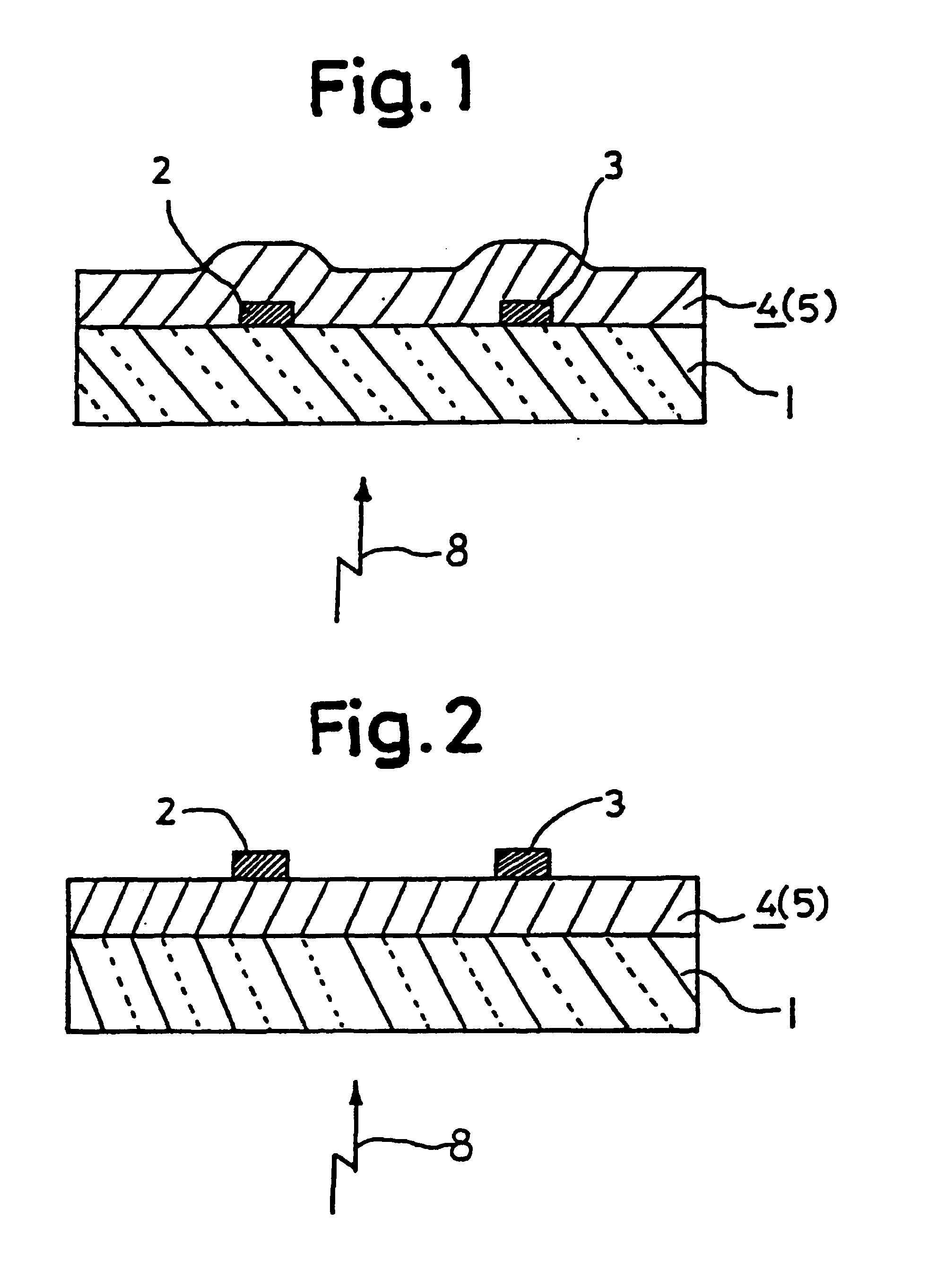
[0040]the semiconductor photo-electrically-sensitive device shown in FIG. 1 has such a construction as follows:

[0041]A light transparent insulating substrate 1 has thereon conductive layers 2 and 3 of, for example, tin oxide. The light transparent substrate 1 is made of glass, fused quartz, synthetic quartz, or the like.

[0042]On the light transparent substrate 1 there is formed a non-single-crystal semiconductor layer member 4. The non-single-crystal semiconductor layer member 4 has an intrinsic non-single-crystal semiconductor layer 5 containing hydrogen or a halogen as a recombination center neutralizer. The intrinsic non-single-crystal semiconductor layer 5 is formed of silicon (Si), germanium (Ge), SixGe1−x, or the like. The layer 5 has a thickness of, for example, 0.5 um.

[0043]The intrinsic non-single-crystal semiconductor layer 5 making up the non-single-crystal semiconductor, layer member 4 is formed by a CVD method which does not employ a glow discharge technique, or a plasm...

second embodiment

[0044]the semiconductor photo-electrically-sensitive device shown in FIG. 2 has such a construction as follows:

[0045]The second embodiment of the semiconductor photo-electrically-sensitive device has the same structure as the first embodiment of the semiconductor photo-electrically-sensitive device shown in FIG. 1 except that the conductive layers 2 and 3 are formed on the non-single-crystal semiconductor layer member 4. Therefore, a detailed description will not be repeated.

third embodiment

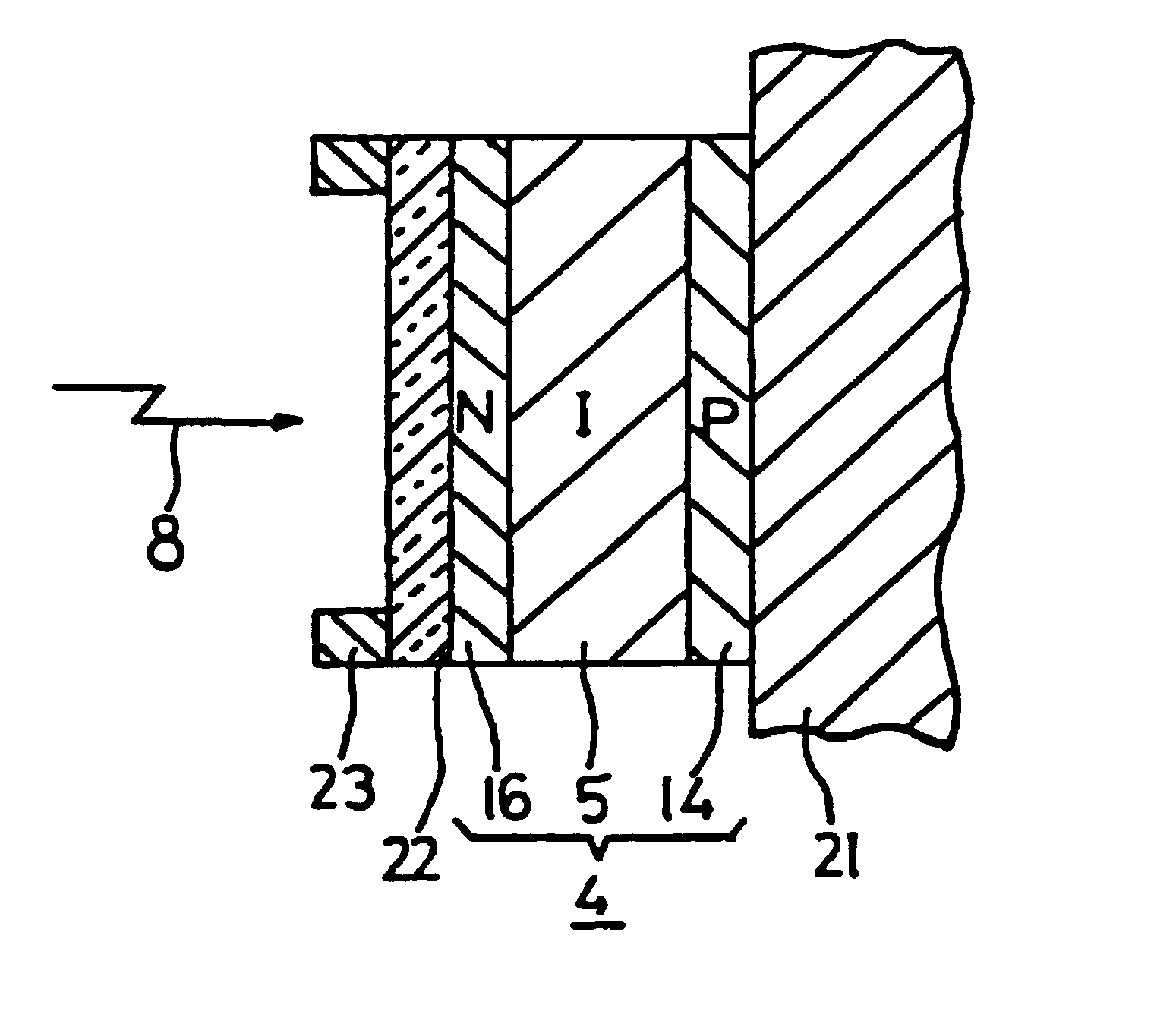
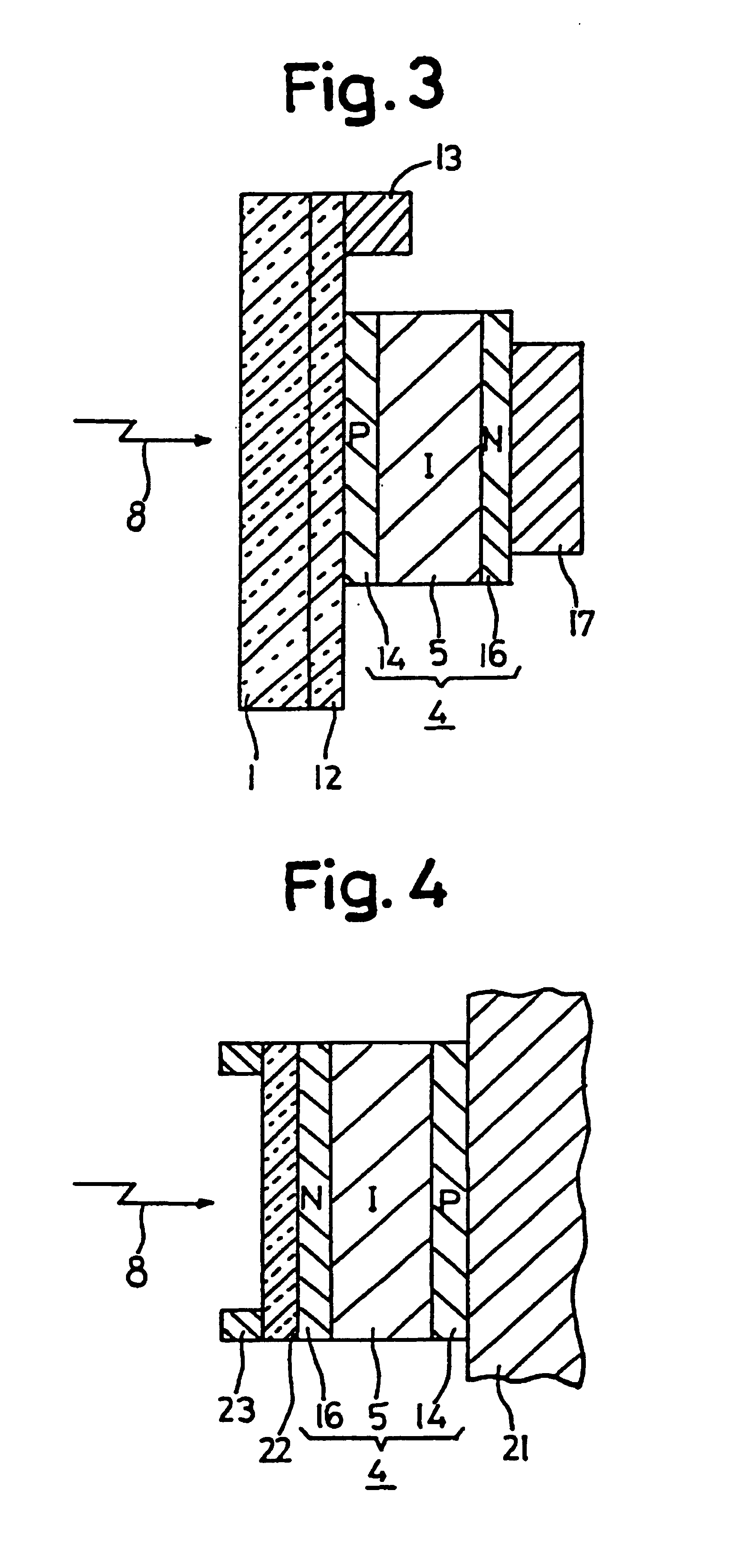
[0046]the semiconductor photoelectric conversion device shown in FIG. 3 has such a construction as follows:

[0047]A light transparent conductive layer 12 of tin oxide is formed, for example, by vacuum deposition on an insulating and light transparent substrate 1 of glass, fused quartz, synthetic quartz, or the like. On the conductive layer 12 there is formed a lead 13 thereof.

[0048]On the light transparent conductive layer 12 there is formed a non-single-crystal semiconductor layer member 4. The non-single-crystal semiconductor layer member 4 is formed by a sequential lamination of, for instance, a P-type non-single-crystal semiconductor layer 14, an intrinsic non-single-crystal semiconductor layer 5 containing hydrogen or a halogen as a recombination center neutralizer, and an N-type non-single-crystal semiconductor layer 16. Accordingly, the non-single-crystal semiconductor layer member 4 has one intrinsic non-single-crystal semiconductor layer 5 and has formed therein one PIN junc...


PUM


Abstract

A semiconductor device including a conductive substrate or a first conductive layer formed on the substrate, a non-single-crystal semiconductor layer member is disposed on the conductive substrate or the conductive layer, the non-single-crystal semiconductor layer member having at least one intrinsic, non-single-crystal semiconductor layer, and a second conductive layer disposed on the non-single-crystal semiconductor layer. The intrinsic non-single-crystal semiconductor layer contains sodium and oxygen in very low concentrations where each concentration is 5×10¹⁸ atoms/cm3 or less.

Description

RELATED APPLICATIONS[0001]This is a Divisional application of Ser. No. 08 / 438,374, filed May 10, 1995 now U.S. Pat. No. 5,556,794; which itself is a divisional of Ser. No. 08 / 350,115, filed Nov. 29, 1994 now U.S. Pat. No. 5,521,400; which itself is a divisional of Ser. No. 07 / 694,406, filed May 1, 1991, now U.S. Pat. No. 5,391,893; which itself is a Continuation-in-Part of Ser. No. 06 / 860,441, filed May 7, 1986, now U.S. Pat. No. 5,043,772.[0002]This application is a Continuation-in-Part of application Ser. No. 06 / 860,441 filed May 7, 1986 which in turn is a Continuation-in-Part of application Ser. No. 06 / 800,694 filed Nov. 22, 1985, now U.S. Pat. No. 4,690,717. This application is also related to application Ser. No. 06 / 525,459 filed Aug. 22, 1983, now U.S. Pat. No. 4,591,892.BACKGROUND OF THE INVENTION[0003]1. Field of the Invention[0004]The present invention relates to improvements in or relating to a semiconductor photo-electrically-sensitive device which has at least a non-sing...

Claims


Application Information

Patent Timeline
Patent Type & Authority Patents(United States)
IPC IPC(8): H01L29/04H01L31/0392
CPCH01L31/0288H01L31/1055H01L31/18Y02E10/50H01L31/1824H01L31/20H01L31/182Y02P70/50
Inventor YAMAZAKI, SHUNPEI
Owner SEMICON ENERGY LAB CO LTD
Why Eureka
Try Eureka