GaN-based field effect transistor of a normally-off type

a field effect transistor and gate electrode technology, applied in the direction of semiconductor devices, semiconductor/solid-state device details, electrical apparatus, etc., can solve the problem of unfavorable electricity consumption of keeping applying the given voltage to the gate electrode, and achieve the effect of greater band gap energy

Inactive Publication Date: 2006-05-02
FURUKAWA ELECTRIC CO LTD
View PDF6 Cites 82 Cited by
  • Summary
  • Abstract
  • Description
  • Claims
  • Application Information

AI Technical Summary

Problems solved by technology

In cases where the HEMT configuration is employed as a switching device for a power source, however, it is unfavorable in terms of electricity consumption to keep applying the given voltage to the gate electrode in order to turn the switch off.

Method used


Image

  • GaN-based field effect transistor of a normally-off type
  • GaN-based field effect transistor of a normally-off type
  • GaN-based field effect transistor of a normally-off type

Examples


embodiment 1

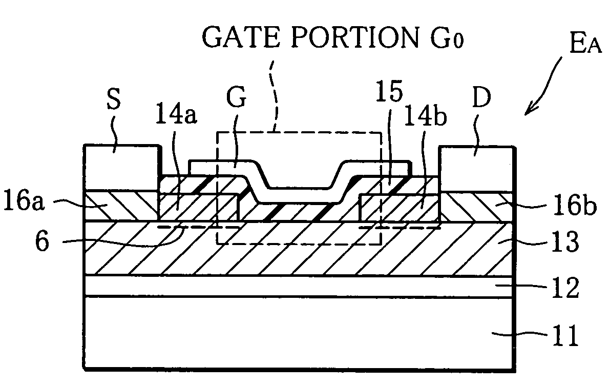
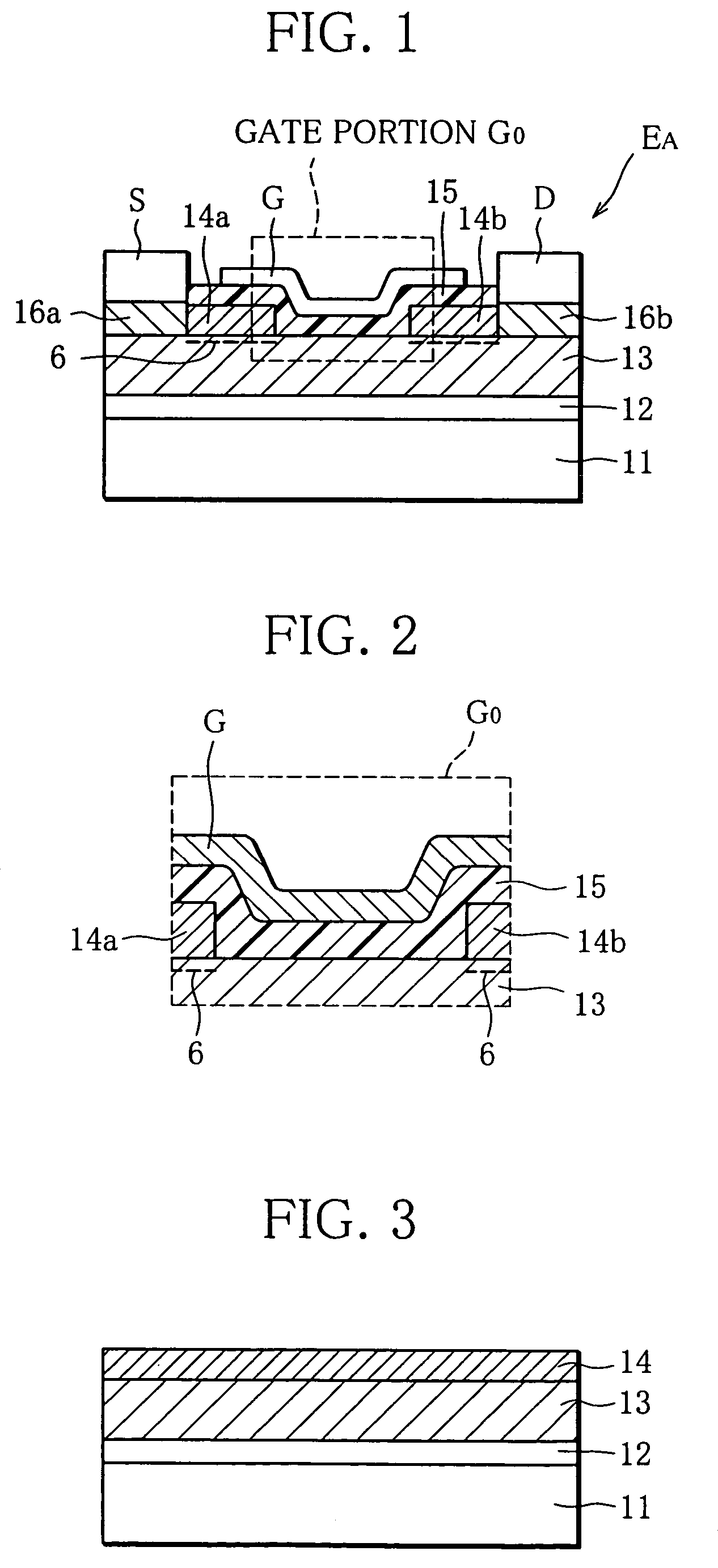
[0125]The GaN-based FET (EA) shown in FIG. 1 was fabricated in the following manner.

[0126]First, as illustrated in FIG. 3, the GaN layer (buffer layer) 12 having a thickness of 50 nm was formed on the sapphire substrate 11 at a growth temperature of 700° C. through the GSMBE method by using nitrogen radical (3×10⁻⁶ Torr) and metal Ga (5×10⁻⁷ Torr). Furthermore, the p-GaN layer 13 (channel layer: carrier concentration is 5×1018 cm−3) having a thickness of 2 μm was formed thereon at a growth temperature of 850° C. by using metal Ga (5×10⁻⁷ Torr), ammonia (5×10⁻⁵ Torr) and metal Mg (5×10⁻⁹ Torr). Subsequently, the undoped Al0.2Ga0.8N layer (electron supply layer) 14 having a thickness of 30 nm was formed thereon at a growth temperature of 850° C. by using metal Al (1×10⁻⁷ Torr), metal Ga (3×10⁻⁷ Torr) and ammonia (5×10⁻⁵ Torr).

[0127]The p-GaN has bandgap energy of 3.4 eV, and the undoped Al0.2Ga0.8N has bandgap energy of 3.94 eV.

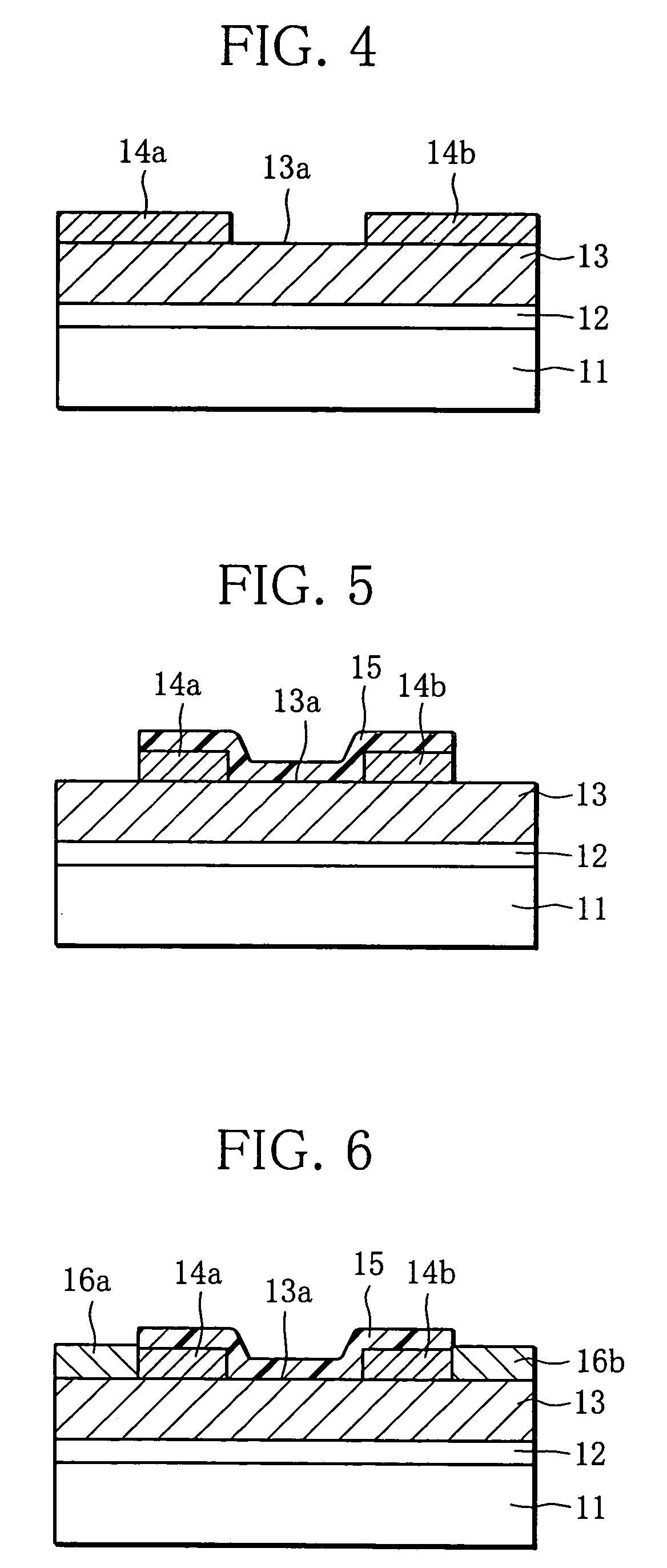
[0128]As illustrated in FIG. 4, the surface was etched us...

embodiment 2

[0132]The GaN-based FET (EC) shown in FIG. 17 was fabricated as described below.

[0133]As illustrated in FIG. 18, the GaN layer (buffer layer) 61 having a thickness of 50 nm was formed at a growth temperature of 700° C. on the sapphire substrate 60 through the GSMBE method by using nitrogen radical (3×10⁻⁶ Torr) and metal Ga (5×10⁻⁷ Torr). Furthermore, the n-GaN layer (contact layer) 54a having a thickness of 30 nm was formed thereon at a growth temperature of 850° C.

[0134]On the contact layer 54a, the p-GaN layer 52c (channel layer: carrier concentration is 5×10¹⁸ / cm3) having a thickness of 2 μm was formed at a growth temperature of 850° C. by using metal Ga (5×10⁻⁷ Torr), ammonia (5×10⁻⁵ Torr) and metal Mg (5×10⁻⁹ Torr). The n-GaN layer (contact layer) 54b having a thickness of 30 nm was formed thereon at a growth temperature of 850° C. by using metal Al (1×10⁻⁷ Torr), metal Ga (3×10⁻⁷ Torr) and ammonia (5×10⁻⁵ Torr).

[0135]Subsequently, as illustrated in FIG. 19, the mask 58a made ...


PUM


Abstract

According to the present invention, there is provided a new GaN-based field effect transistor of a normally-off type, which has an extremely small ON resistance during operation and is capable of a large-current operation. The GaN-based field effect transistor according to the present invention comprises source and drain electrodes; a channel portion made of a first GaN-based semiconducting material that is an i-GaN-based semiconducting material or a p-GaN-based semiconducting material, the channel portion being so formed as to be electrically connected to the source and drain electrodes; first and second electron supply portions made of a second GaN-based semiconducting material having greater bandgap energy than the first GaN-based semiconducting material, the first and second electron supply portions being joined to the channel portion and located separately from each other; an insulating layer formed on the surface of the channel portion, which spreads between the first and second electron supply portions; and a gate electrode disposed on the insulating layer.

Description

TECHNICAL FIELD[0001]The present invention relates to a GaN-based field effect transistor, and more specifically to a new GaN-based field effect transistor of a normally-off type, which has an extremely small ON resistance during operation and is capable of a large-current operation.BACKGROUND ART[0002]GaN-based semiconducting materials including GaN, InGaN, AlGaN, AlInGaN and the like have greater bandgap energy than GaAs-based materials and the like. Moreover, GaN-based semiconducting materials have a high heat resistance, thereby being excellent in a high-temperature operation. Therefore, development research in various kinds of devices which take advantage of the above-mentioned characteristics of GaN-based semiconducting materials, has been proceeded by using GaN, especially.[0003]An example of a GaN-based HEMT configuration is shown in FIG. 33.[0004]In this HEMT configuration, there is formed on a semi-insulating substrate 91, such as a sapphire substrate, a heterojunction str...

Claims


Application Information

Patent Timeline
Patent Type & Authority Patents(United States)
IPC IPC(8): H01L31/0328H01L21/335H01L29/20H01L29/778
CPCH01L29/66462H01L29/7789H01L29/7787H01L29/7788H01L29/778H01L29/2003
Inventor YOSHIDA, SEIKOHSASAKI, MASAYUKI
Owner FURUKAWA ELECTRIC CO LTD
Why Eureka
Try Eureka