Organic light emitting diode display

a light-emitting diode and display technology, applied in the field of organic light-emitting diode displays, can solve the problems of reducing the life of the display, luminance of the display, and reducing the ambient contrast ratio

Inactive Publication Date: 2006-05-02
GLOBAL OLED TECH
View PDF9 Cites 59 Cited by
  • Summary
  • Abstract
  • Description
  • Claims
  • Application Information

AI Technical Summary

Problems solved by technology

Conventional OLED displays have limited ambient contrast ratio and limited luminance.
OLED displays have the problem that their ambient contrast ratio is greatly decreased when used in bright ambient illumination (due primarily to reflection of the ambient illumination from the face or substrate of the display).
The luminance of an OLED display can be increased by increasing the current density flowing through the OLED light emissive materials, but doing so reduces the lifetime of the display, increases the power usage, and decreases the efficiency of the display.
Moreover, at these higher currents, the power usage of the OLED displays is no longer competitive with back-lit LCD displays.
However, this approach does not increase the efficiency of the display and the increased power usage of the display may not be competitive with alternative display technologies, such as LCDs.
However, these approaches still fail to meet the minimum ambient contrast ratio required for indoor and outdoor viewing.
This approach is not compatible with the current manufacturing techniques used to make active matrix OLED displays, since for top emitting OLED display devices, a layer of thin film transistors are formed on the substrate prior to forming the OLEDs.
The use of photoresist to create plasmon inducing gratings is problematical because the photoresist is an electrical insulator, thereby isolating the underlying ITO conductors from the OLED materials.
The use of shadow masks is not practical to create the gratings because of the small dimensions of the gratings.
They also disclose that they have fabricated an OLED that uses surface plasmon coupling on a silicon substrate, but silicon substrates are not conventional or practical for OLED display devices.

Method used


Image

  • Organic light emitting diode display
  • Organic light emitting diode display
  • Organic light emitting diode display

Examples


Embodiment Construction

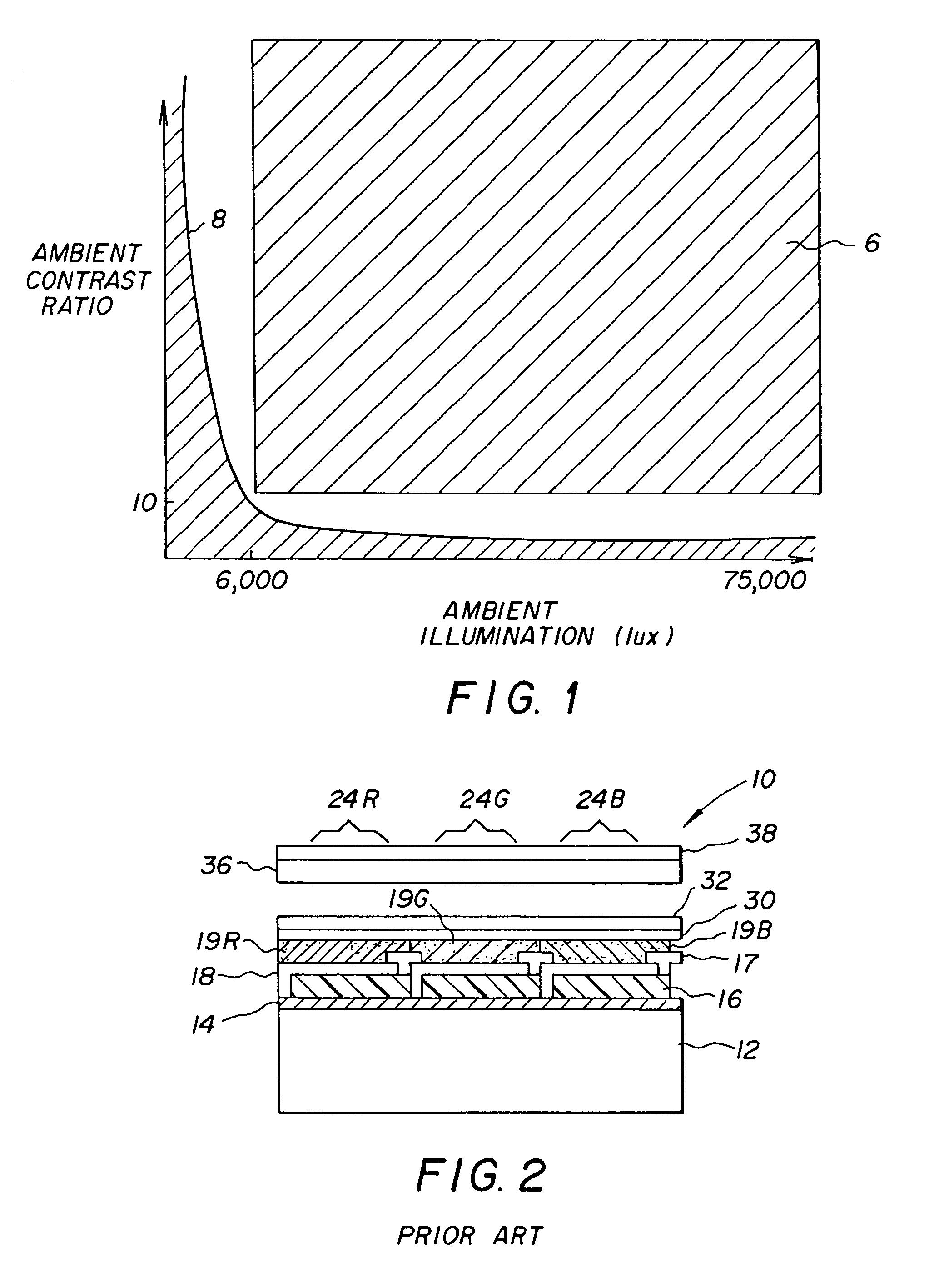
[0020]An OLED display according to the present invention has an ambient contrast ratio greater than ten in an ambient illumination greater than 6,000 lux at an average power of 100 milliwatts or less per square centimeter of display area. Referring to FIG. 1, the shaded area of the graph labeled 6 represents the operating ranges of display devices according to the present invention. Prior art OLED display devices operate in the range labeled 8.

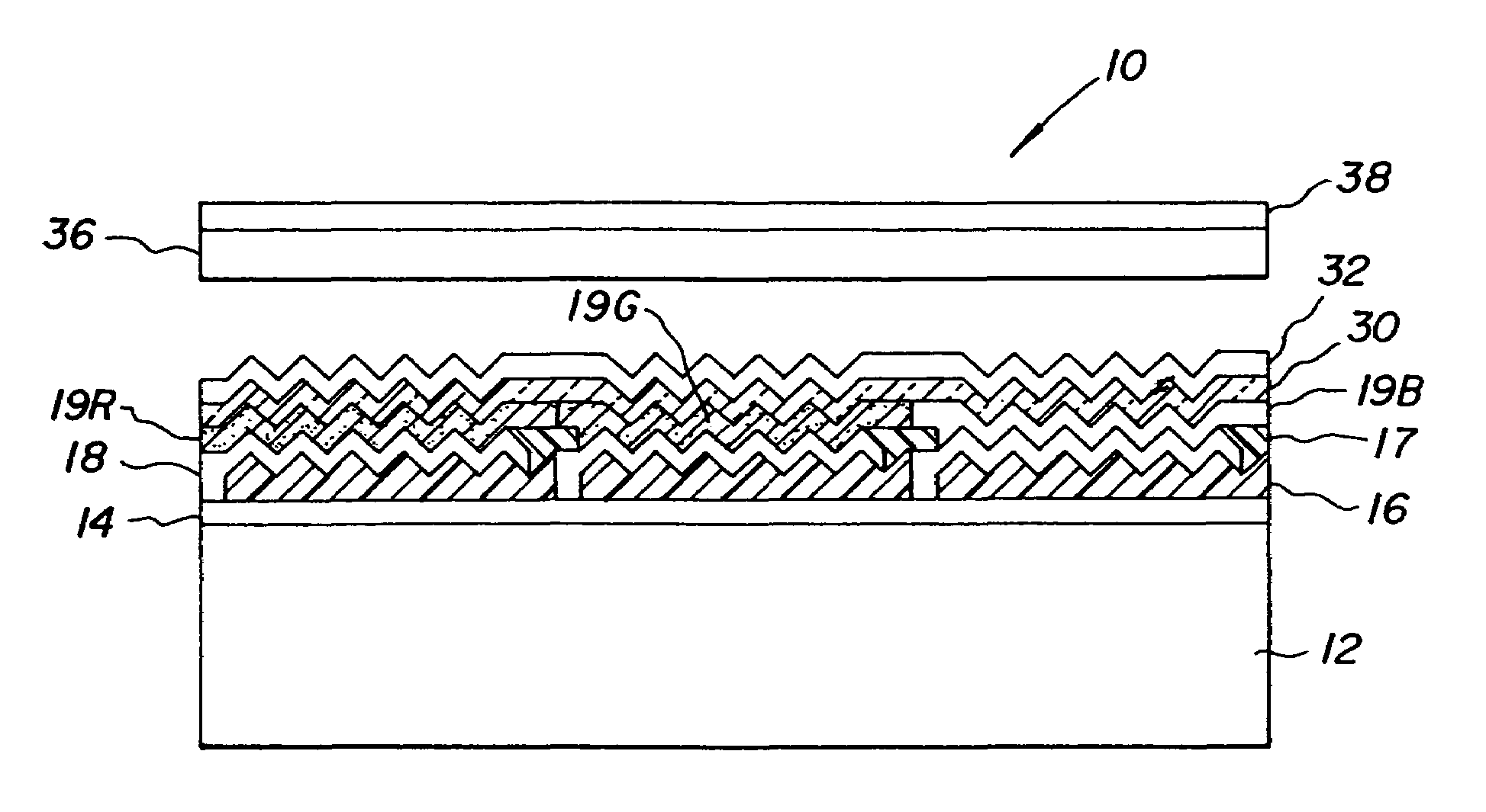
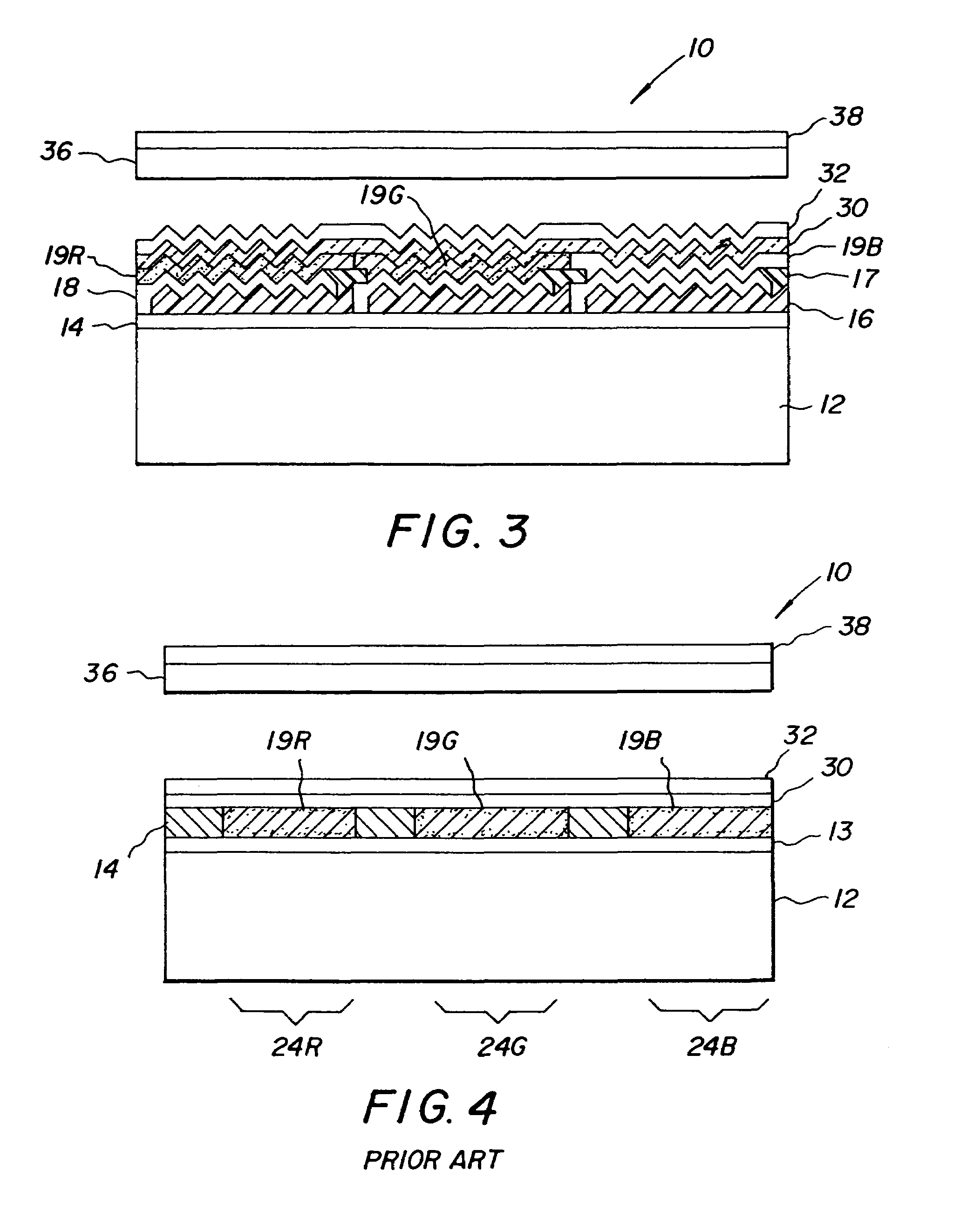
[0021]Referring to FIG. 2, a prior art top-emitting OLED display device 10 includes a substrate 12, and a thin-film transistor (TFT) active matrix layer 14 comprising an array of TFTs that provides power to OLED elements. A patterned first insulating layer 16 is provided over the TFT active matrix layer, and an array of first electrodes 18 are provided over a planarized insulating layer 16 and in electrical contact with the TFT active matrix layer. A patterned second insulating layer 17 is provided over the array of first electrodes 18 such th...


PUM

PropertyMeasurementUnit
reflectanceaaaaaaaaaa
heightsaaaaaaaaaa

Abstract

An OLED display having an ambient contrast ratio greater than ten at an ambient illumination greater than 6,000 lux at an average power of 100 milliwatts per centimeter squared.

Description

FIELD OF THE INVENTION[0001]The present invention relates to organic light emitting diode displays, and more particularly to their use in high-ambient illumination conditions.BACKGROUND OF THE INVENTION[0002]Flat-panel displays of various sizes are used widely for many computing and communication applications. In particular, flat-panel displays are used in both indoor and outdoor applications under a wide variety of ambient lighting conditions. For adequate visibility displays require an ambient contrast ratio of at least three for viewing text and at least 10 for viewing images or graphics, where ambient contrast ratio (ACR) is defined as:[0003]ACR=1+PDLADR×AI(1)where PDL is the peak display luminance in lumens per meter squared; ADR is percent average display reflectance; and AI is the ambient illumination in lux[0004]Indoor applications experience relatively low levels of ambient illumination and require lower levels of display luminance to achieve the required ambient contrast r...

Claims


Application Information

Patent Timeline
Patent Type & Authority Patents(United States)
IPC IPC(8): H01J1/62H01L51/50H01L27/32H01L51/00H01L51/30H01L51/52H05B33/02H05B33/26
CPCH01L51/529H01L51/5262H01L51/5281H01L27/3244H01L51/0038H01L51/005H01L51/0059H01L51/0081H01L51/5278H01L51/0077H10K59/12H10K85/114H10K85/60H10K85/631H10K85/30H10K85/324H10K50/85H10K50/19H10K50/87H10K50/86
Inventor ARNOLD, ANDREW D.COK, RONALD S.
Owner GLOBAL OLED TECH
Why Eureka
Try Eureka