Method for actuating a transistor

a transistor and actuation method technology, applied in the direction of logic circuit coupling/interface arrangement, pulse technique, instruments, etc., can solve the problems of low immunity to interference, inability to use, and unreliable switching operations, and achieve reliable switching operations, simple switching structures, and high immunity to interference.

Inactive Publication Date: 2006-05-09
INFINEON TECH AG
View PDF6 Cites 4 Cited by
  • Summary
  • Abstract
  • Description
  • Claims
  • Application Information

AI Technical Summary

Benefits of technology

[0004]It is therefore an object of the present invention to provide an actuation method for an electronic switching device which permits a high level of immunity to interference and reliable switching operations with a simple switching structure.

Problems solved by technology

The problem with such circuits, however, is that they cannot be used if the potential difference between the positive digital supply voltage and the negative digital supply voltage exceeds the breakdown voltage of the electronic switching devices used, according to their specification.
Another drawback of the conventional circuit type is low immunity to interference and unreliable switching operations when too low a digital supply voltage is provided in comparison with the threshold voltage of the switching device used.
The aforementioned drawbacks may be removed by providing additional negative supply voltages and by using stepped or cascaded level converters, but this makes the circuit very complex and requires additional negative supply voltages.

Method used


Image

  • Method for actuating a transistor
  • Method for actuating a transistor
  • Method for actuating a transistor

Examples


Embodiment Construction

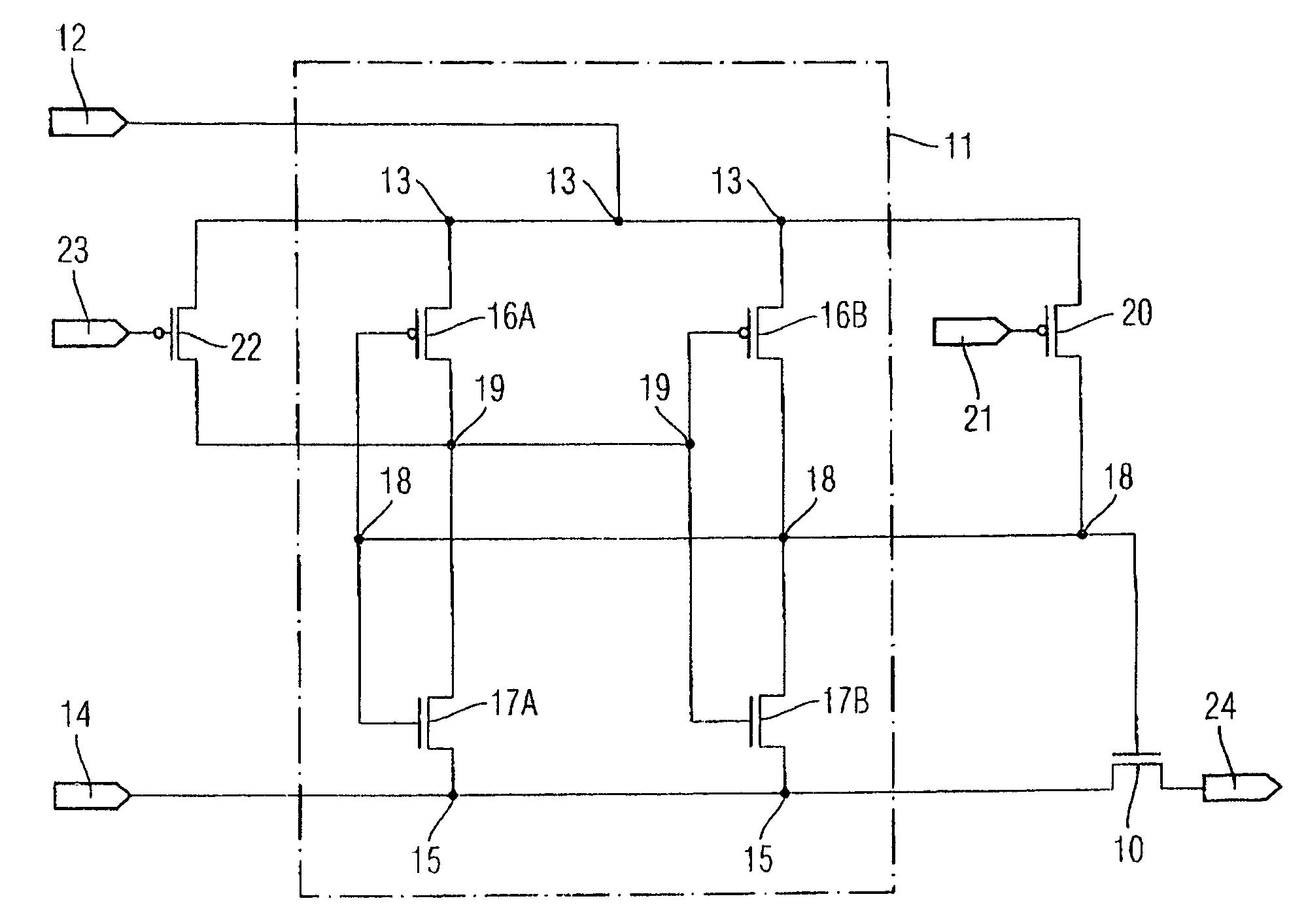
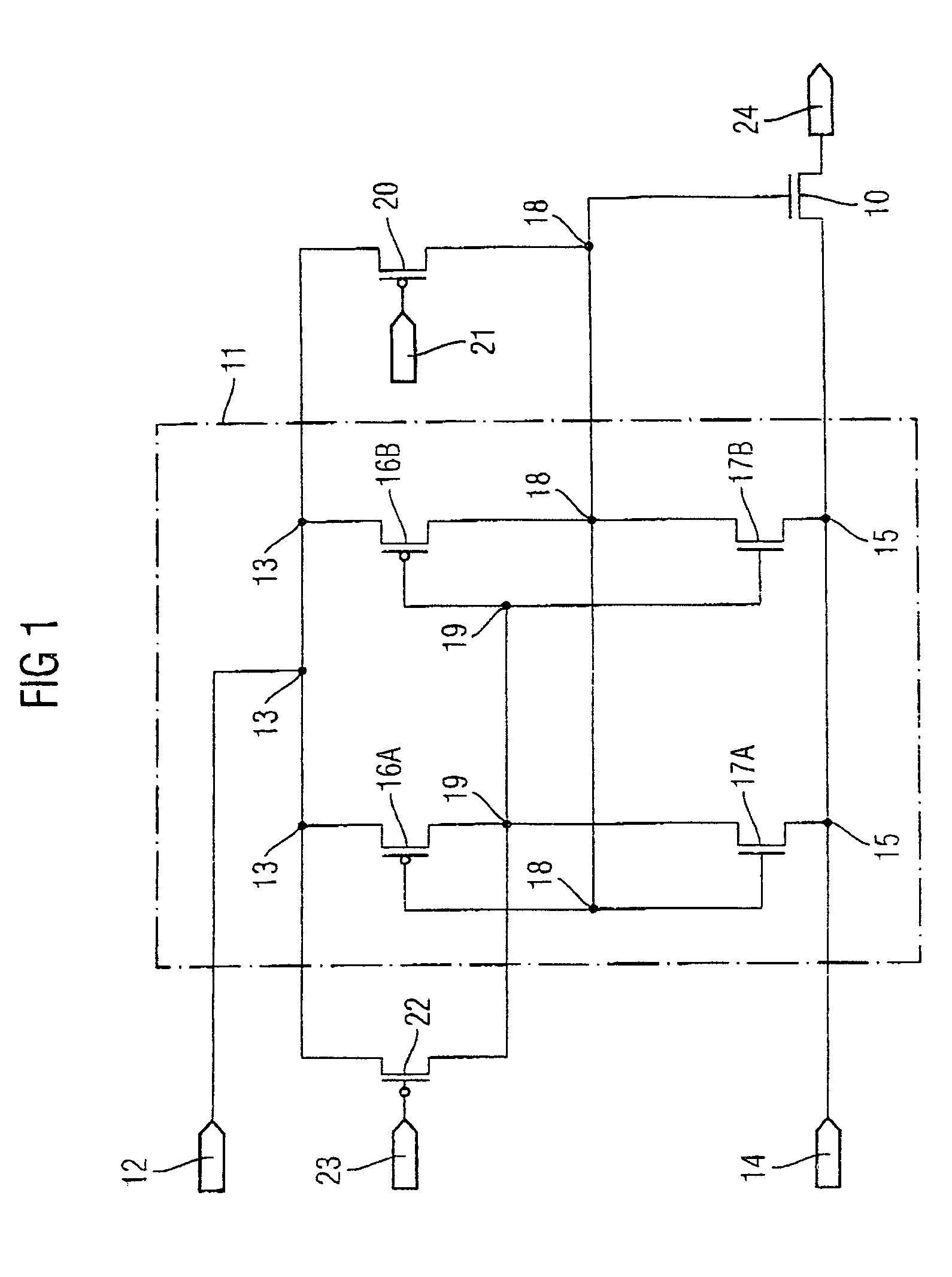
[0022]In the figures, identical reference symbols denote parts which are the same or have the same function.

[0023]FIG. 1 shows a schematic actuation circuit in an electronic switching device 10, preferably in an NMOS transistor. In line with FIG. 1, the actuation circuit in the electronic switching device 10 has a latch circuit 11. The latch circuit 11 has a first voltage supply input 12, which is connected to a first voltage supply node 13. In addition, the latch circuit 11 has a second voltage supply input 14, which is connected to a second voltage supply node 15. The first voltage supply node 13 is used to apply a potential between a predetermined positive potential and a reference-ground potential. The second voltage supply node 15 is used to provide a potential in a range between the reference-ground potential and a predetermined negative potential. The second voltage supply node 15 is connected to the source of the transistor 10.

[0024]Between the first voltage supply node 13 a...


PUM


Abstract

The present invention provides a method for actuating a transistor (10) having the following steps: (a) a first predetermined positive potential is applied to a first voltage supply node (13) in a latch circuit (11), the voltage supply node (13) being coupled to a control connection on the transistor (10); (b) a reference-ground potential is applied to a second voltage supply node (14) in the latch circuit (11), the second voltage supply node (14) being connected to a source connection on the transistor (10); (c) the latch circuit (11) is set to a predetermined state, which turns the transistor (10) on or off; (d) the potential at the second voltage supply node (14) is lowered; and (e) the potential at the first voltage supply node (13) is lowered if the potential difference between the first and second voltage supply nodes (13, 14) exceeds a predetermined threshold value.

Description

TECHNICAL FIELD[0001]The present invention relates to a method for actuating a transistor, and particularly to an actuation method for a transistor with a negative switching voltage, actuated using a latch structure.BACKGROUND ART[0002]For applications in which negative switching voltages are required, appropriate actuation voltages need to be generated for electronic switching devices, such as switching transistors. An NMOS switch requires a voltage range which extends from a negative voltage for ensuring good isolation to a predetermined voltage above this negative switched voltage, in order to permit a low forward resistance for the switching transistor.[0003]Known switching assemblies use circuits which effectively switch digital levels, such as a reference-ground potential as available positive digital supply voltage and a negative voltage supply potential as negative digital supply voltage. The problem with such circuits, however, is that they cannot be used if the potential d...

Claims


Application Information

Patent Timeline
Patent Type & Authority Patents(United States)
IPC IPC(8): H03K3/356H03K17/06
CPCH03K17/063
Inventor JANKOWSKI, MACIEJROGL, STEPHAN
Owner INFINEON TECH AG
Why Eureka
Try Eureka