Write circuit of double data rate synchronous DRAM

a write circuit and data rate technology, applied in the field of write circuits of double data rate synchronous dram, can solve the problems of skew generation all the time, difficult voltage and temperature in real conditions, and almost impossible to satisfy the condition td=0, and achieve the effect of stable data write operation

Active Publication Date: 2006-05-09
MOSAID TECH
View PDF11 Cites 87 Cited by
  • Summary
  • Abstract
  • Description
  • Claims
  • Application Information

AI Technical Summary

Benefits of technology

[0023]The present invention is directed to a write circuit of a DDR SDRAM, which is capable of performing a stable data write operation even at a very high frequency by detecting a skew between a clock and a data strobe signal during a write operation of the DDR SDRAM and compensating timing difference between signals.
[0025]To accomplish the above objects, the present invention suggests to move a position where clock domain crossing occurs to a write driver and to use the delay of an input data strobe falling signal dsf for a certain amount of time as input data strobe bar signals dinstb_e and dinstb_o, thereby ensuring that a proper data is always transferred to a gio bus line. Moreover, a timing margin between a clock and a data strobe is much increased by using a skew detector to detect a skew tDQSS between a clock and a data strobe and automatically compensating the skew tDQSS through a skew compensation circuit using a direct synchronous mirror delay type DLL (Delay Locked Loop).

Problems solved by technology

As a result of this, a skew is generated all the time.
However, optimizing the skew against all changes in process, voltage and temperature is not always easy in real conditions.
In reality, however, it is almost impossible to satisfy the condition td=0 because of changes in process, voltage and temperature.
Also, as the operation frequency gets higher, the skew td of input data strobe signals dinstb_e and dinstb_o for the output data from the multiplexer should be controlled within an extremely small range, which, in reality, is a very difficult task to accomplish.

Method used


Image

  • Write circuit of double data rate synchronous DRAM
  • Write circuit of double data rate synchronous DRAM
  • Write circuit of double data rate synchronous DRAM

Examples


Embodiment Construction

[0053]The following detailed description will present a preferred embodiment of the invention in reference to the accompanying drawings.

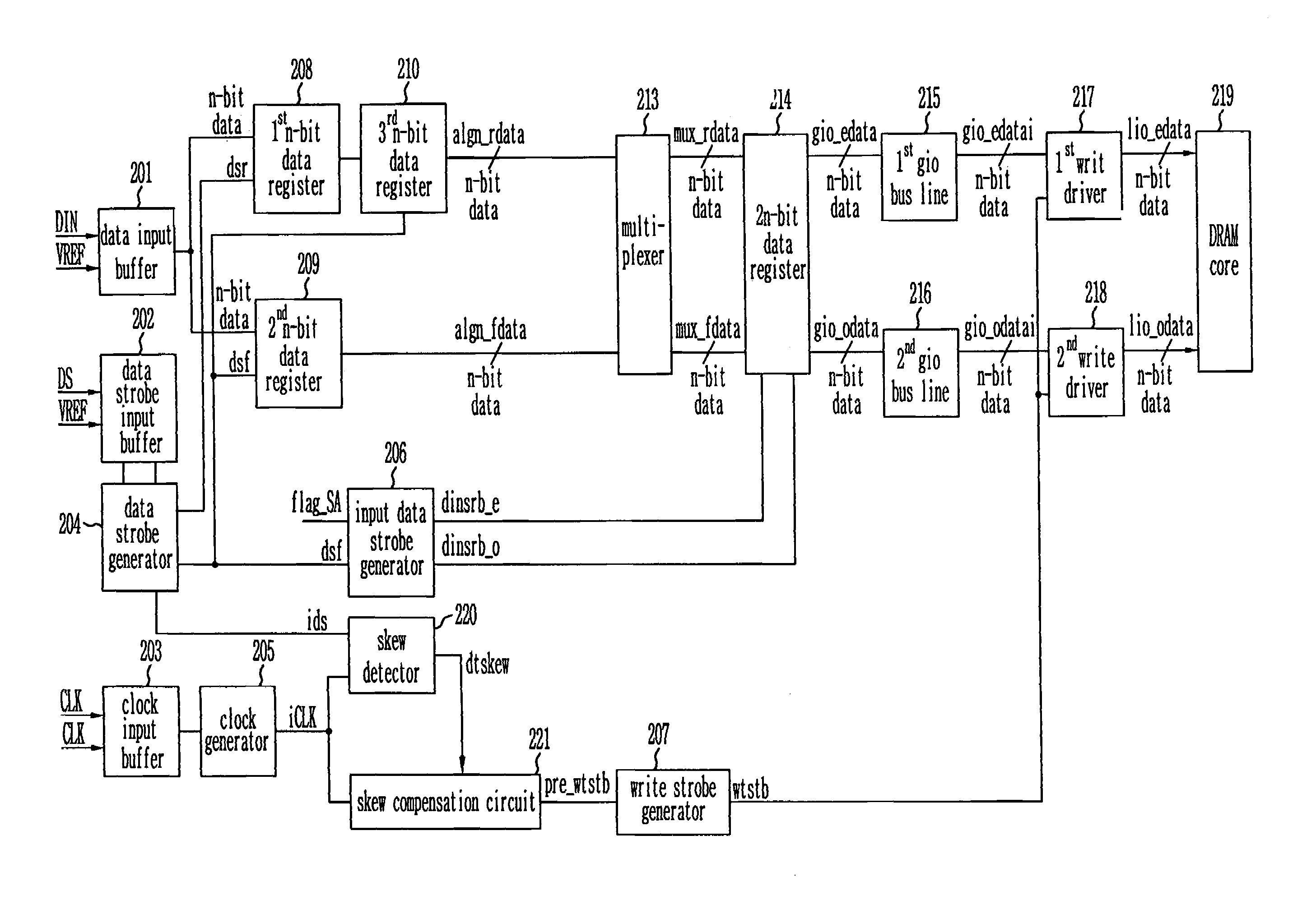
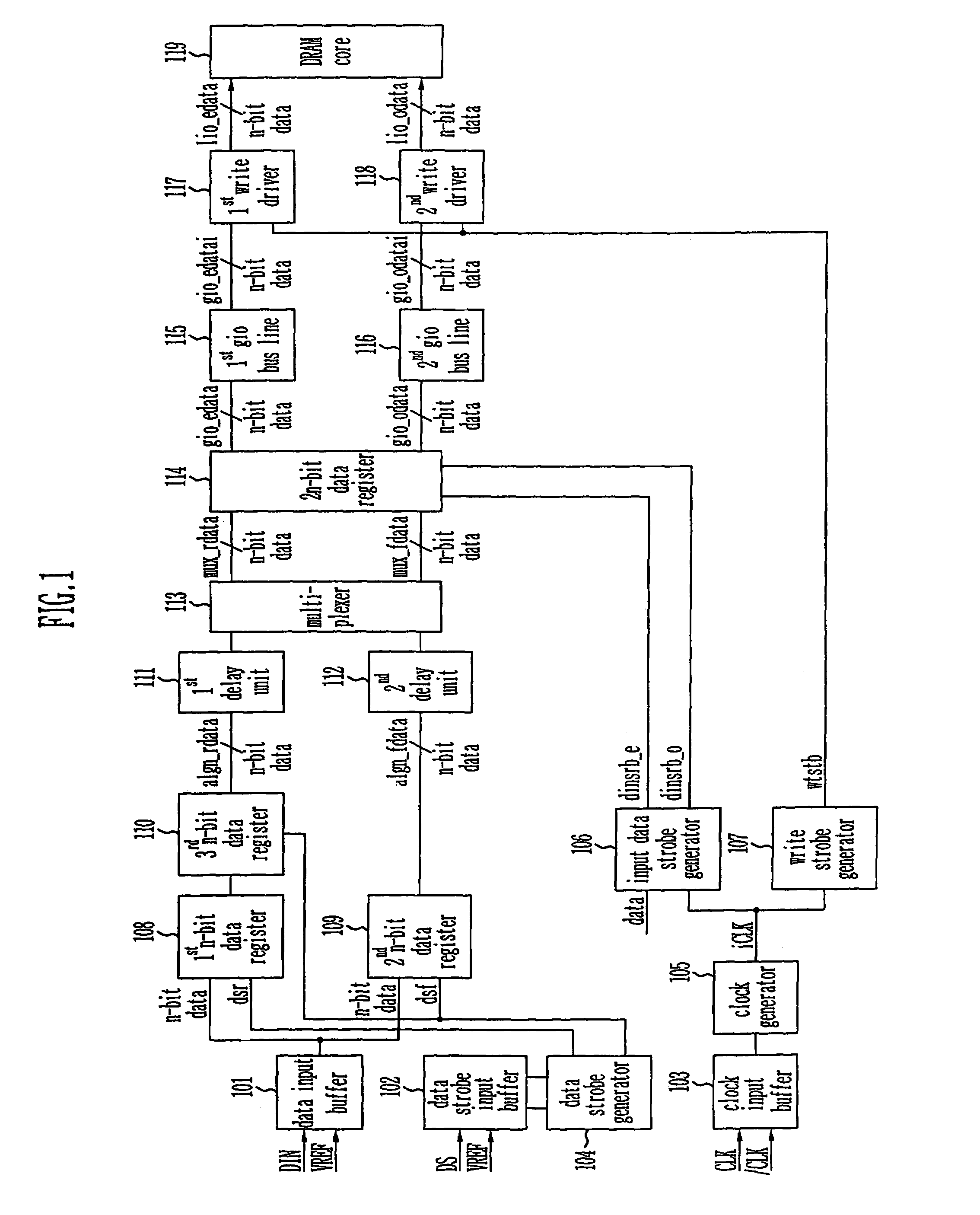
[0054]FIG. 5 is a block diagram in relation to a write operation of a DDR SDRAM according to the present invention. There are several differences between the structure of the related art DDR SDRAM of FIG. 1 and that of the DDR SDRAM of the present invention. First of all, input data strobe signals dinstb_e and dinstb_o are not generated by an internal clock iCLK but by an internal data strobe ids, so different kinds of clock domain crossing are not generated at a 2n-bit data register. In fact, the clock domain crossing is generated at a write driver. Also, a write strobe wtstb, with an aid of a skew detector and a skew compensation circuit, generates a pre write strobe pre_wtstb without a tDQSS skew after a certain time of delay. Particularly, a direct synchronous mirror delay type DLL (Delay Locked Loop) used for the skew compensation circuit is a ...


PUM


Abstract

Provided is a write circuit of a DDR SDRAM, in which a clock domain crossing is generated from a writing driver during a data write operation and a proper data is always transferred to a gio bus line by using the delay of an internal data strobe signal's falling for a certain amount of time as an input data strobe bar signal. Moreover, by using a skew detection circuit, it is possible to detect a skew tDQSS between a clock and a data strobe, and the skew tDQSS is automatically compensated by the skew compensation circuit. From the perspective of a timing error between the clock and the data strobe, therefore, the write operation of the DDR SDRAM has twice the timing margin (0.5tCK) compared to that of the related art. This means that a stable, high-speed write operation of the DDR SDRAM can be made possible.

Description

[0001]This application relies for priority upon Korean Patent Application No. 2003-0100162 filed on Dec. 30, 2003, the contents of which are herein incorporated by reference in their entirety.BACKGROUND[0002]1. Field of the Invention[0003]The present invention relates in general to a write circuit of a Double Data Rate Synchronous DRAM (DDR SDRAM), and more particularly, to a write circuit of a DDR SDRAM, in which a clock domain crossing is generated from a writing driver during a data write operation and a proper data is always transferred to a gio bus line by using the delay of an internal data strobe signal's falling for a certain amount of time as an input data strobe bar signal, and at the same time, time is compensated when a skew is generated between a clock signal and a data strobe signal, thereby realizing a high-speed operation of a memory device.[0004]2. Discussion of Related Art[0005]Recently, a lot of attention has been paid to an interface with an external device to ke...

Claims


Application Information

Patent Timeline
Patent Type & Authority Patents(United States)
IPC IPC(8): G11C8/00G11C7/10G11C11/40
CPCG11C7/1072G11C7/1096G11C7/1093G11C7/1078G11C11/40
Inventor CHO, YONG DEOK
Owner MOSAID TECH
Why Eureka
Try Eureka