Quartz damage repair method for high-end mask

a high-end, quartz-based technology, applied in the field of quartz-based damage repair methods, can solve the problems of affecting the definition of exposed patterns, bad and unusable masks, time-consuming and expensive, etc., and achieves the elimination of concerns about opaque material peeling, high repair accuracy, and easy control

Inactive Publication Date: 2006-05-16
TAIWAN SEMICON MFG CO LTD
View PDF4 Cites 6 Cited by
  • Summary
  • Abstract
  • Description
  • Claims
  • Application Information

AI Technical Summary

Benefits of technology

[0018]Another objective of the invention is to provide a method of repairing photolithographic exposure masks that has high accuracy of repair.
[0019]Yet another objective of the invention is to provide a method of repairing photolithographic exposure masks that eliminates concerns of peeling of opaque material after the repair has been performed.
[0020]In accordance with the objectives of the invention a new method is provided for repairing photolithographic exposure masks. The invention uses an etch function of a conventional mask repair tool. The invention addresses defects that occur in a pattern of opaque material (such as chrome) created over the surface of an exposure mask whereby an (undesired) opening exists in the opaque material. The invention uses a focused ion-beam exposure of the surface of the exposure mask to purposely “damage” this surface over the area where the opaque material is required to be present. Repair accuracy is in this manner easy to control, the conventional problem of peeling of the opaque or light sensitive material is eliminated.

Problems solved by technology

In these Phase Shifting Masks (PSM) the projected light that is in extreme close physical proximity is mutually interactive, having a detrimental effect on the definition of the exposed pattern.
Due to the frequently used high density of the pattern that is developed in the layer of opaque material, this formation is exposed to a number of problems that result in bad and unusable masks.
In view of the density and the potential complexity of the pattern that has been created on the substrate of the photo mask, this process however can be cumbersome, time consuming and expensive.

Method used


Image

  • Quartz damage repair method for high-end mask
  • Quartz damage repair method for high-end mask
  • Quartz damage repair method for high-end mask

Examples


Embodiment Construction

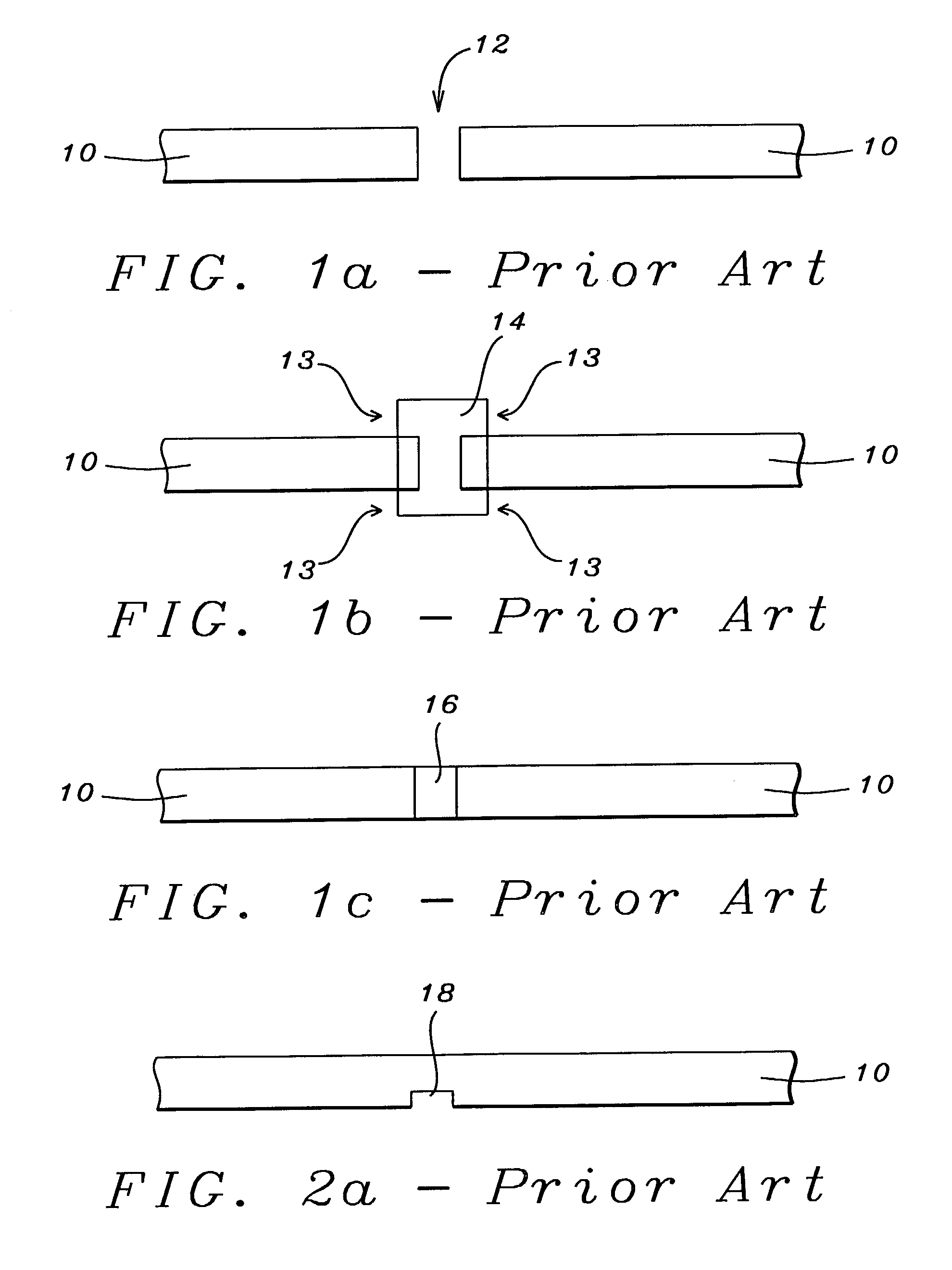
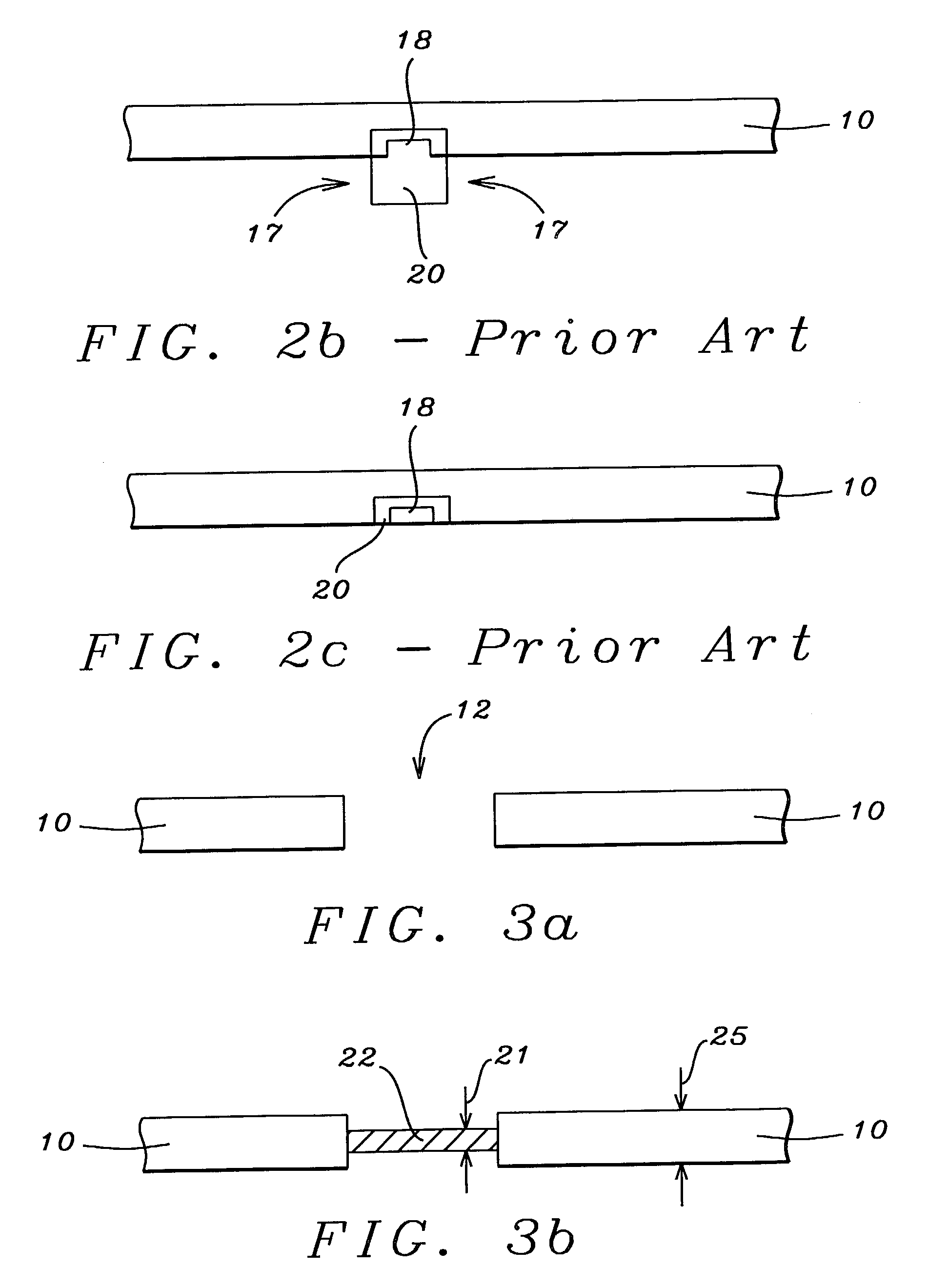
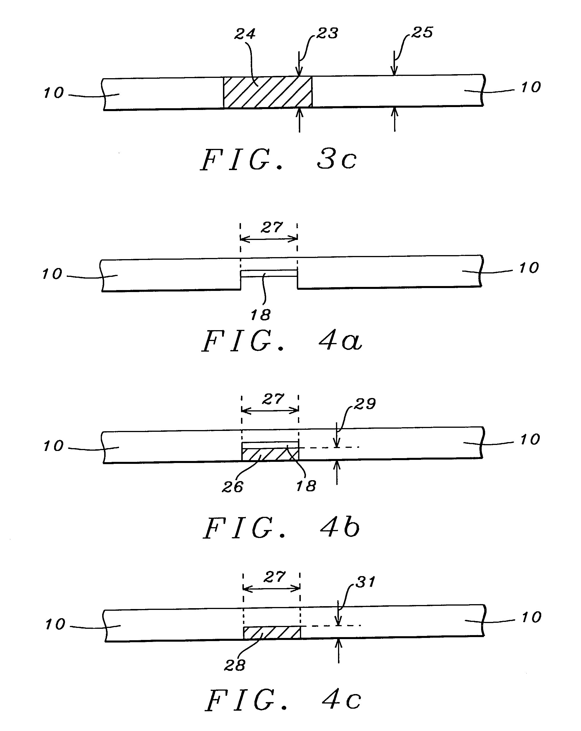
[0027]Required improvements in semiconductor product performance can only be achieved by designing devices having smaller device dimensions. The smaller dimensions that are required for advanced semiconductor devices can only be achieved if these smaller dimensions are reflected in the photolithographic imaging masks that are used to create the device features of reduced dimensions. Photolithographic masks must therefore be designed having on the surface thereof smaller and higher-density patterns. This brings with it that repair of a pattern on the surface of an exposure mask is more difficult when using conventional methods and tools of repair for exposure masks that are used for the creation of advanced, deep sub-micron semiconductor devices.

[0028]Typical repairs of a chromium or phase shift mask address two problems that are experienced with these mask, that is clear defects in which portions of the light-absorbing chromium are missing and opaque defect or defects of intrusion i...


PUM

PropertyMeasurementUnit
thicknessaaaaaaaaaa
Depthaaaaaaaaaa
Depthaaaaaaaaaa

Abstract

A method is provided for repairing photolithographic exposure masks. A focused ion-beam exposure of the surface of the exposure mask is used to purposely “damage” this surface over the area where opaque or light-blocking material is required to be present.

Description

[0001]This application is a Continuation-in-Part of Ser. No. 10 / 134,822 (now U.S. Pat. No. 6,555,277, issued Apr. 29, 2003), filing date Apr. 26, 2002.BACKGROUND OF THE INVENTION[0002](1) Field of the Invention[0003]The invention relates to the fabrication of integrated circuit devices, and more particularly, to a method of repairing high-end quartz masks.[0004](2) Description of the Prior Art[0005]One of the most essential components that is used during the process of performing photolithographic exposures is a photomask that contains patterns that need to be transposed from the mask to underlying layers of semiconductor material such as most notably the surface of a layer of photoresist. The standard mask comprises a transparent substrate on the surface of which a patterned layer of opaque material has been created. Typically used for the opaque material is chromium that has been deposited over the quartz substrate to a thickness of about 1,000 Angstroms.[0006]Alternate opaque mat...

Claims


Application Information

Patent Timeline
Patent Type & Authority Patents(United States)
IPC IPC(8): G03F9/00G03C5/00G03F1/00
CPCG03F1/72
Inventor CHEN, SAME-TINGLIN, ZY YING
Owner TAIWAN SEMICON MFG CO LTD
Why Eureka
Try Eureka