Inductor element

a technology of inductor elements and elements, applied in the direction of impedence networks, inductances, multiple-port networks, etc., can solve the problems of ineffective functioning of inductor elements, difficult to form high-frequency circuits, and interrupt the flow of effective magnetic flux generated by inductor conductors, so as to reduce manufacturing costs, simplify manufacturing processes, and reduce manufacturing costs

Inactive Publication Date: 2006-05-16
RICOH KK
View PDF9 Cites 99 Cited by
  • Summary
  • Abstract
  • Description
  • Claims
  • Application Information

AI Technical Summary

Benefits of technology

[0010]In particular, when the substrate described above is a semiconductor substrate, it is desirable to form the capacitor where a device constant can be changed by a variable capacitance diode. While it becomes possible to miniaturize parts by using the variable capacitance diode formed with using the semiconductor substrate, it becomes possible to reduce a manufacturing cost by simplifying manufacturing process in comparison with the case where external parts are attached thereafter, and wiring etc. are performed. Similarly, when the substrate described above is a semiconductor substrate, it is desirable to form a variable resistor made of an FET whose channel is used as a resistor. While it is possible to miniaturize parts by using the variable resistor made of the FET formed with using the semiconductor substrate, it becomes possible to reduce a manufacturing cost by simplifying manufacturing process in comparison with the case where external parts are attached thereafter, and wiring etc. are performed.
[0011]In addition, it is desirable to form an inductor, which constitutes the impedance element, by a conductive layer formed on the substrate in predetermined shape. Since high Q is not required of the inductor used for terminating the end of a conductor, it is possible to realize the inductor with a conductor pattern on the substrate. Moreover, since it becomes possible to form this conductor pattern at the same process with using a metal layer for performing various kinds of wiring etc., it becomes possible to perform miniaturization of parts, simplification of process, and cost reduction.
[0012]In addition, it is desirable to form two conductors, described above, in the substantially same shape or long shape. Since an upper conductor never directly faces the front side of the substrate owing to making the two conductors the same in shapes, it is possible to reduce the eddy currents that are generated on the substrate when the upper conductor directly faces the substrate. In addition, it is possible to give predetermined inductance to the upper conductor by making the shapes of the two conductors be long. In particular, since it is possible to give large inductance to a conductor when the conductor is formed in one or more turns of spiral shape or a meander shape, the conductor is suitable for being built in a comparatively low frequency circuit. In addition, since it is possible to give a small inductance to a conductor when the conductor is formed in a circular shape less than one turn or an substantially linear shape in comparison with the case where the conductor is formed in a spiral shape or the like, the conductor is suitable for being built in a comparatively high frequency circuit.
[0013]In addition, when the shape is a spiral one having one or more turns, it is necessary to extend a lead wire from the inner circumferential end of the inductor conductor having this spiral shape. Nevertheless, it is possible to suppress to the minimum the interruption of flow of the effective magnetic flux, generated by the inductor conductor, by leading out the lead wire between the conductor, being near the substrate, and the substrate.

Problems solved by technology

Nevertheless, since eddy currents are induced on the front side of the semiconductor substrate by this magnetic flux to cancel effective magnetic flux, there is a problem of not effectively functioning as the inductor element.
In particular, the higher a frequency of a signal that flows in the inductor element becomes, the more remarkable this inclination becomes, and hence it is difficult to form a high-frequency circuit, containing an inductor element, on a semiconductor substrate.
Hence there is a possibility of interrupting the flow of effective magnetic flux generated by the inductor conductor depending on the configuration of lead wires extended from the inductor conductor.
Therefore, there is an issue that sufficient characteristics cannot be obtained.
In addition, since the floating conductor is in the state where it floats thoroughly electrically, in this floating conductor, unnecessary reflection may arise depending on a frequency and the like of a signal outputted from or inputted to the inductor conductor.
Hence there is a possibility that sufficient characteristics are not obtained depending on circumstances.

Method used


Image

  • Inductor element
  • Inductor element
  • Inductor element

Examples


first embodiment

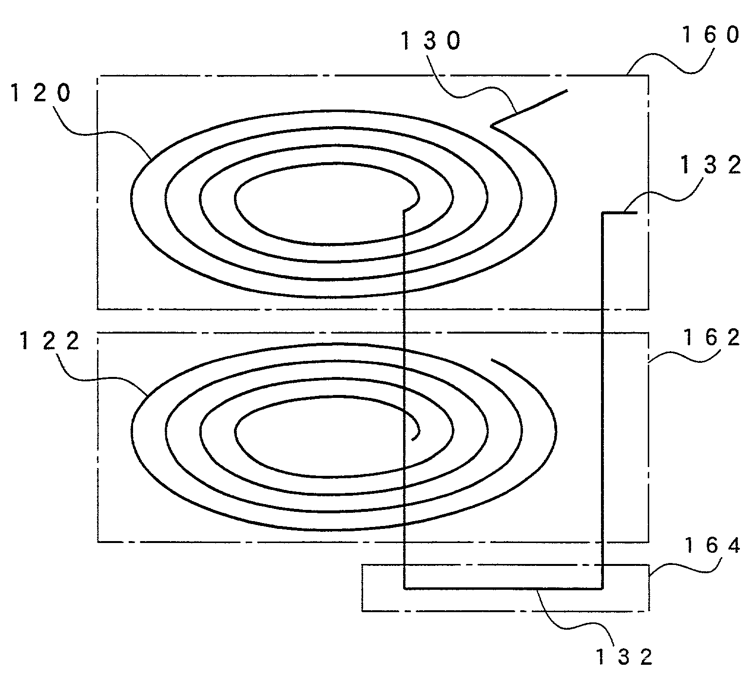
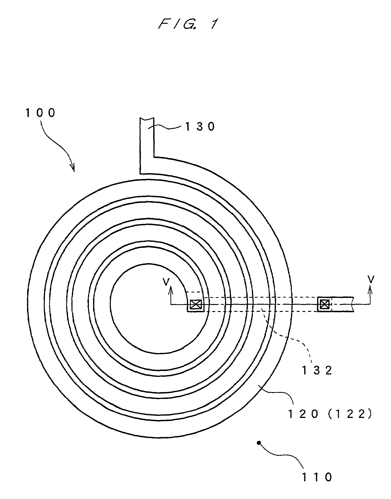
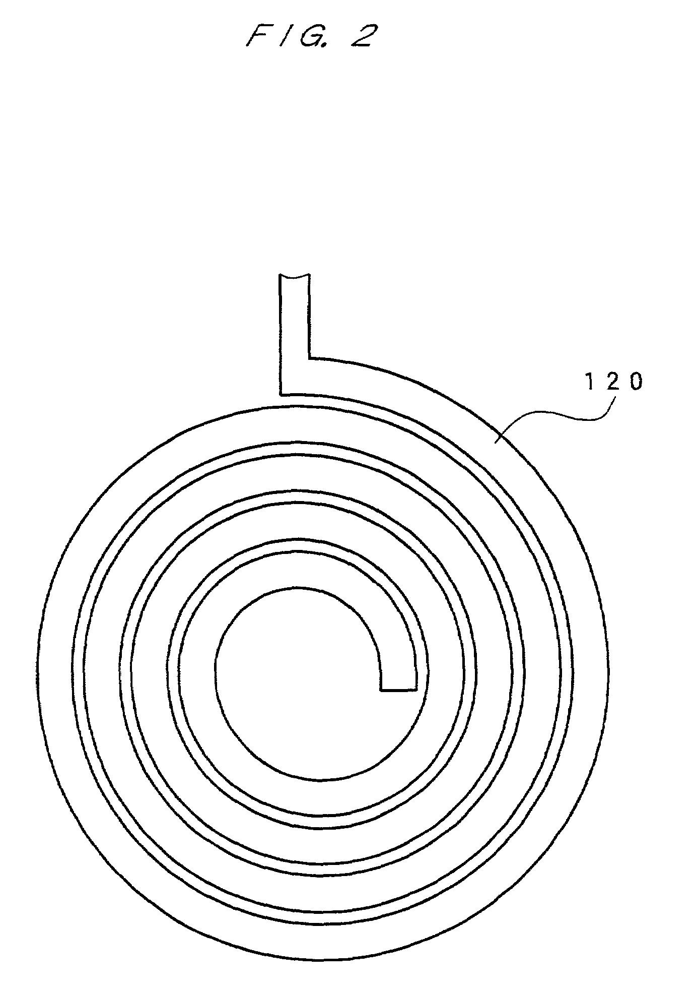
[0028]FIG. 1 is a schematic diagram showing a planar structure of an inductor element according to the first embodiment. In addition, FIG. 2 is a drawing showing an upper layer of conductor included in the inductor element shown in FIG. 1. FIG. 3 is a drawing showing a shape of a lower layer of conductor included in the inductor element shown in FIG. 1.

[0029]An inductor element 100 according to this embodiment has two conductors 120 and 122 that have spiral shapes and are formed on the surface of a semiconductor substrate 110. These two conductors 120 and 122 have substantially the same shape. When viewed from the front side of the semiconductor substrate 110, they are formed so that the conductor 120, which becomes an upper layer, and another conductor 122, which becomes a lower layer, are formed by being superimposed one on the other substantially exactly. Each of the conductors 120 and 122 is formed of, for examples, a thin film of metal (metal layer), or semiconductor material s...

second embodiment

[0036]FIG. 6 is a diagram showing the structure of an inductor element 100A in a second embodiment. This is different in that a predetermined impedance element 200 is added to the inductor element 100 in the first embodiment shown in FIG. 4.

[0037]Namely, in the inductor element 100 in the first embodiment described above, with paying attention to the other conductor 122 located so as to substantially superimpose the one conductor 120 serving as an inductor conductor, both ends are free (open state). In this embodiment, the characteristics of the whole inductor element 100A can be improved or adjusted by terminating the inner circumferential end of the conductor 122 through the impedance element 200.

[0038]For example, when electric current flows into the one conductor 120 of the inductor element 00A, induced current flows to the other conductor 122. However, it becomes possible to prevent unnecessary reflection in this inner circumferential end by terminating the inner circumferentia...


PUM

PropertyMeasurementUnit
shapeaaaaaaaaaa
shapesaaaaaaaaaa
circular shapesaaaaaaaaaa

Abstract

An inductor element having good characteristics is formed on a substrate. An inductor element 100 includes two spiral conductors 120, 122 formed on the surface of a semiconductor substrate 110. The upper conductor 120 and the lower conductor 122 have substantially the same shape, and the conductor 120 is used as an inductor conductor, while the conductor 122 is used as a floating conductor. The outer and inner ends of the conductor 120 are connected with lead wires 130, 132, respectively, and the lead wire 132 connected with the inner ene extends outside between the lower conductor 122 and the semiconductor substrate 110.

Description

TECHNICAL FIELD[0001]The present invention relates to an inductor element that is formed on various kinds of substrates such as a semiconductor substrate.BACKGROUND ART[0002]There is known such a semiconductor circuit that forms a spiral pattern electrode on a semiconductor substrate with using thin film forming technique and uses this pattern electrode as an inductor element. If current flows in such an inductor element that is formed on such a semiconductor substrate, magnetic flux is generated in the direction perpendicular to the spiral pattern electrode. Nevertheless, since eddy currents are induced on the front side of the semiconductor substrate by this magnetic flux to cancel effective magnetic flux, there is a problem of not effectively functioning as the inductor element. In particular, the higher a frequency of a signal that flows in the inductor element becomes, the more remarkable this inclination becomes, and hence it is difficult to form a high-frequency circuit, cont...

Claims


Application Information

Patent Timeline
Patent Type & Authority Patents(United States)
IPC IPC(8): H01F5/00H01F17/00H01L21/822H01L23/522H01L27/04H03H7/075
CPCH01F17/0006H01F17/0013H01L23/522H01L23/5227H01L2924/12044H01L2924/0002H01L2924/3011H01L2924/00H01F2017/0073
Inventor OKAMOTO, AKIRAIKEDA, TAKESHI
Owner RICOH KK
Why Eureka
Try Eureka