
Actuatable diffractive optical processor

a technology of optical processors and diffractive optical components, applied in the field of optical processors, can solve the problems of limited useable portion of the surface, limited dynamic range, and limitations in optical performance, and achieve the effects of improving the planarity of the grating elements, reducing insertion loss, and increasing dynamic rang

Inactive Publication Date: 2006-05-16
AHURA SCI +1
View PDF92 Cites 11 Cited by
  • Summary
  • Abstract
  • Description
  • Claims
  • Application Information

AI Technical Summary

Benefits of technology

[0015]Exemplary aspects of this invention include optical processors that eliminate the gaps between grating elements, while providing improved planarity of the grating elements during actuation of the optical processor's grating elements. Accordingly, embodiments of these exemplary aspects have reduced insertion loss, and increased dynamic range. Still other exemplary aspects of the invention provide reduced power consumption, and reduced cost of production of optical processors.

Problems solved by technology

If precise positioning is not maintained over the entire surface of the optical processor, the useable portion of the surface is limited to the portions that are precisely positioned.
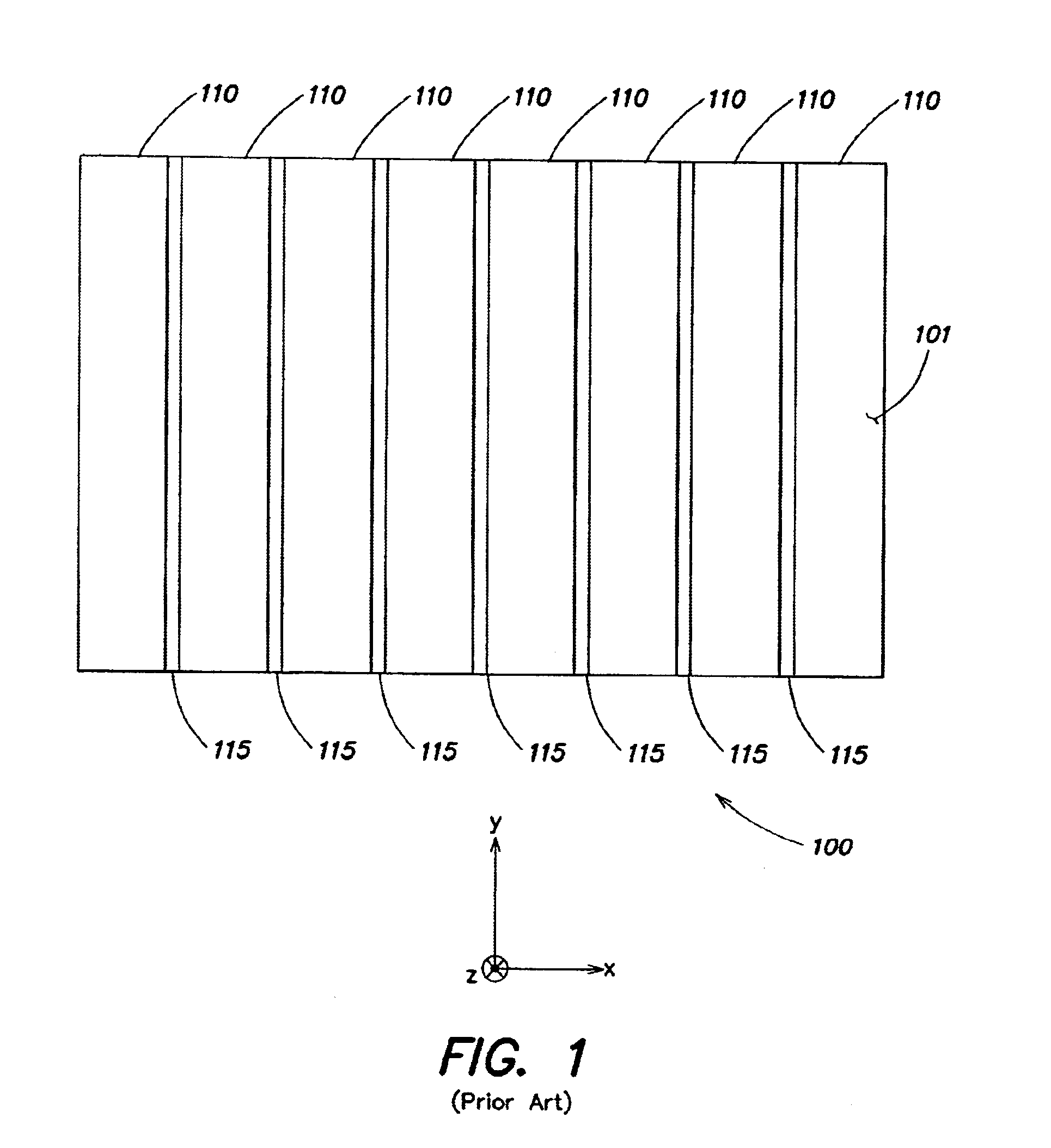
Other MEMS grating structures have allowed the grating elements to remain nearly planar during actuation, but structures necessary to maintain planarity have resulted in limitations in optical performance. FIG. 1 is a schematic top view of a MEMS diffractive optical processor 100 that illustrates a basic topography for prior art MEMS diffractive optical processors that maintains planarity of the grating elements during actuation.
Accordingly, prior art MEMS-based optical processors having such a topography have had limitations in insertion loss, and dynamic range.

Method used


Image

  • Actuatable diffractive optical processor
  • Actuatable diffractive optical processor
  • Actuatable diffractive optical processor

Examples


Embodiment Construction

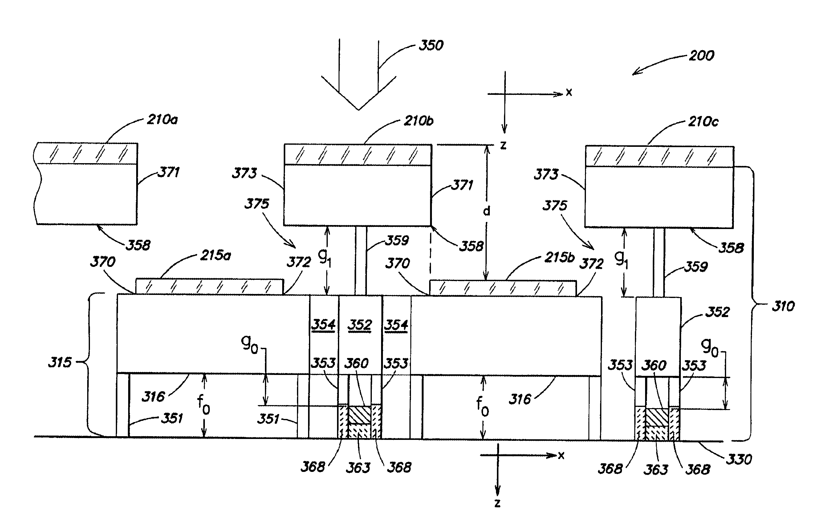
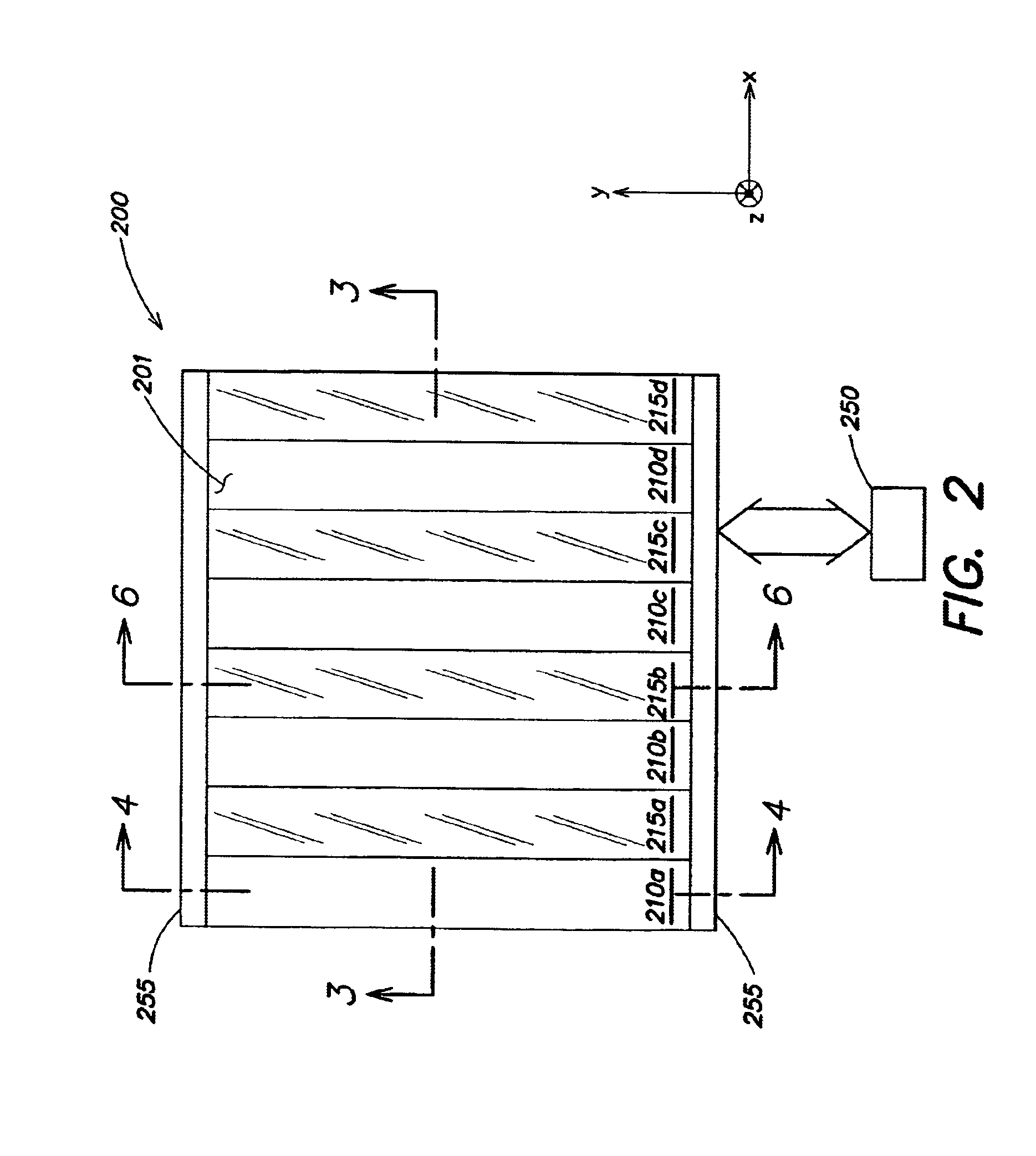
[0031]FIG. 2 is a top view of one example of one embodiment of an electrostatically-actuatable diffractive optical processor 200 according to the present invention. FIG. 3 is a cross-sectional side view of the diffractive optical processor of FIG. 2 taken along the line 3—3 that illustrates exemplary mirror surfaces 210a-c and 215a-b. Top surface 201 of optical processor 200 includes upper mirror surfaces 210a-d (collectively referred to as 210) and lower mirror surfaces 215a-d (collectively referred to as 215). Upper mirror surfaces 210 and lower mirror surfaces 215 have elongate dimensions in direction-y and widths in direction-x.

[0032]Although the upper mirror surfaces 210a-d and lower mirror surfaces 215a-d do not form a planar or continuous surface in direction-x, the phrase “top surface” will be used herein to refer to the upper mirror surfaces 210a-d and lower mirror surfaces 215a-d. In one embodiment of optical processor 200, the ends of upper mirror surfaces 210 and lower m...


PUM


Abstract

A programmable MEMS diffractive optical processor having actuatable grating elements that are optically adjacent and supported at points intermediate the ends of the grating elements. The grating elements are maintained substantially flat during actuation of the grating elements.

Description

BACKGROUND OF THE INVENTION[0001]1. Field of Invention[0002]This invention relates to optical processors and more particularly to actuatable, diffractive optical processors.[0003]2. Related Art[0004]Microelectromechanical manufacturing techniques facilitate batch fabrication of microelectromechanical systems (or “MEMS”) that have complex features and functions. Microscale sensing and actuation applications are particularly well addressed by MEMS.[0005]For many MEMS applications, electrostatically-actuated structures are particularly effective as analog positioning and tuning components. Electrostatic actuation provides a combination of advantages for the microscale size regime of MEMS, including the ability to produce high energy densities and large force generation, as well as high operational speed, and the general ease of fabrication.[0006]Electrostatic actuation of a structure is typically accomplished by applying a voltage between an electrode on the structure and an electrode ...

Claims


Application Information

Patent Timeline
IPC IPC(8): G02B26/08
CPCG02B26/0808B82Y30/00
Inventor DEUTSCH, ERIK R.SMITH, MALCOLM C.BUTLER, MICHAEL A.SENTURIA, STEPHEN D.
Owner AHURA SCI
Learn More