LED packaging structure

a technology of led packaging and led components, applied in the direction of sustainable manufacturing/processing, final product manufacturing, semiconductor/solid-state device details, etc., can solve the problems of reducing the competitive power of products, affecting the competitiveness of products, and affecting the product yield

Active Publication Date: 2006-05-23
HARVATEK CORPORATION
View PDF2 Cites 35 Cited by
  • Summary
  • Abstract
  • Description
  • Claims
  • Application Information

AI Technical Summary

Benefits of technology

[0008]It is a first object of the present invention to provide an LED packaging structure, in which two holes are formed on a substrate thereof and two conductors extend respectively through the two holes to connect electrically to the conductive elements on the upper and lower surfaces of the substrate, whereby the LED packaging structure is easily fabricated.
[0009]It is a second object of the present invention to provide an LED packaging structure, in which the conductors extend through the holes of a substrate thereof and the conductive elements on the upper and lower surfaces of the substrate are separated from the edges of the substrate by a certain interval, thereby avoiding short-circuits of adjacent LED packaging structures due to contact therebetween.
[0011]The substrate has two holes through the upper and lower surfaces, two conductors extending respectively along the two holes such that one of the conductors is electrically connected at both of its terminals to the conductive pad and the first electrode pad, respectively, and the other conductor is electrically connected at both of its terminals to the conductive strip and the second electrode pad, respectively. Therefore, fabrication thereof is easy, and short-circuits of adjacent LED packaging structures due to contact of conductive elements thereof can be avoided.

Problems solved by technology

However, since the large-area substrate may be obliquely cut during the slicing process, this results in irregular half-circle side walls, thereby decreasing product yield.
Moreover, when a plurality of LED packaging structures are aligned in a matrix arrangement for use of display device, and two adjacent packaging structures are positioned close and thus may contact each other (as shown in FIG. 2), the half-circle side walls and the electrode pads of the adjacent LED packaging structures may be positioned close to and be in contact with each other, thereby resulting in a short-circuit.
As a result, assembly and fabrication take longer and are more expensive, thereby leading to the degradation of the competitive power of the products.

Method used


Image

  • LED packaging structure
  • LED packaging structure
  • LED packaging structure

Examples


Embodiment Construction

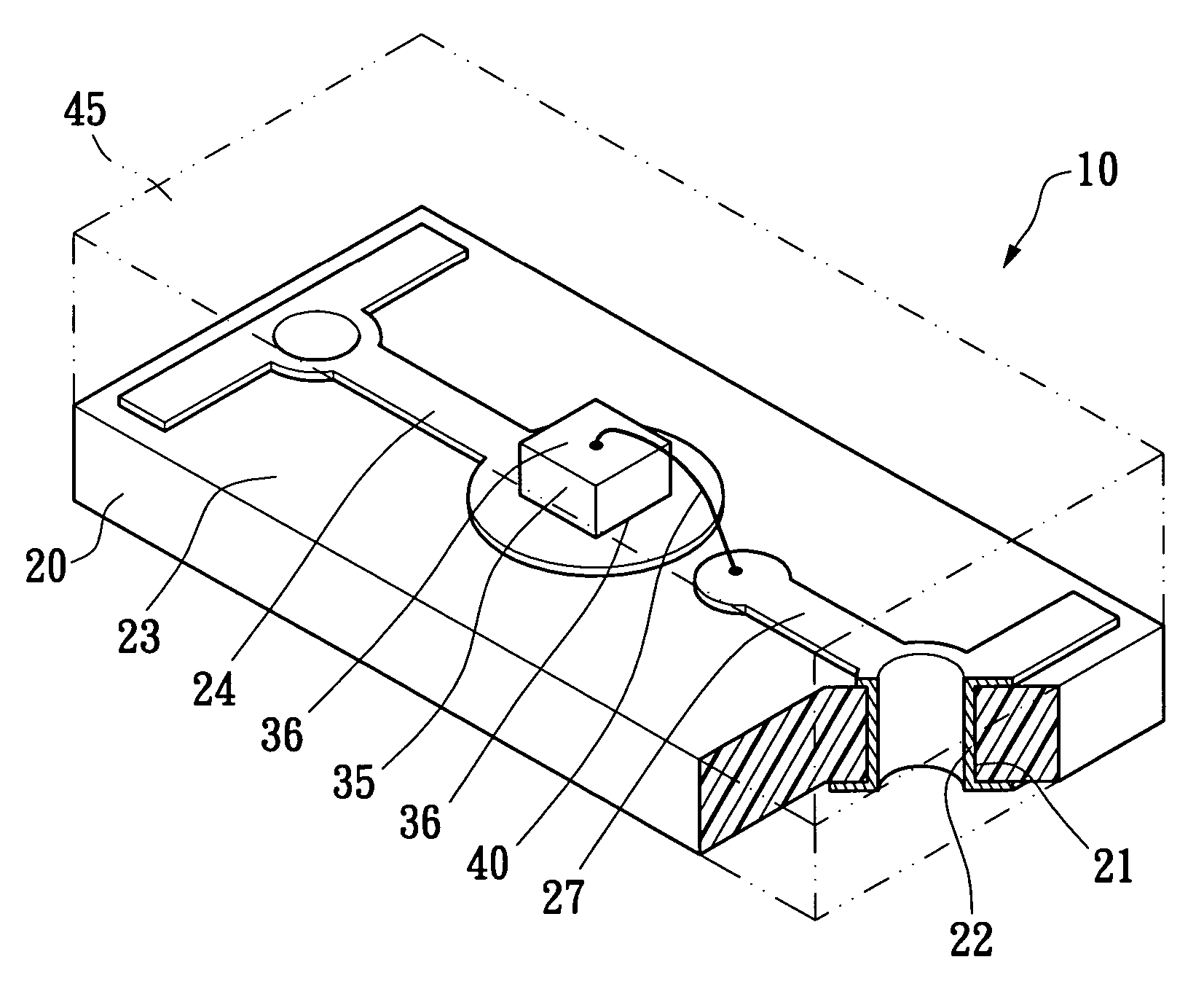
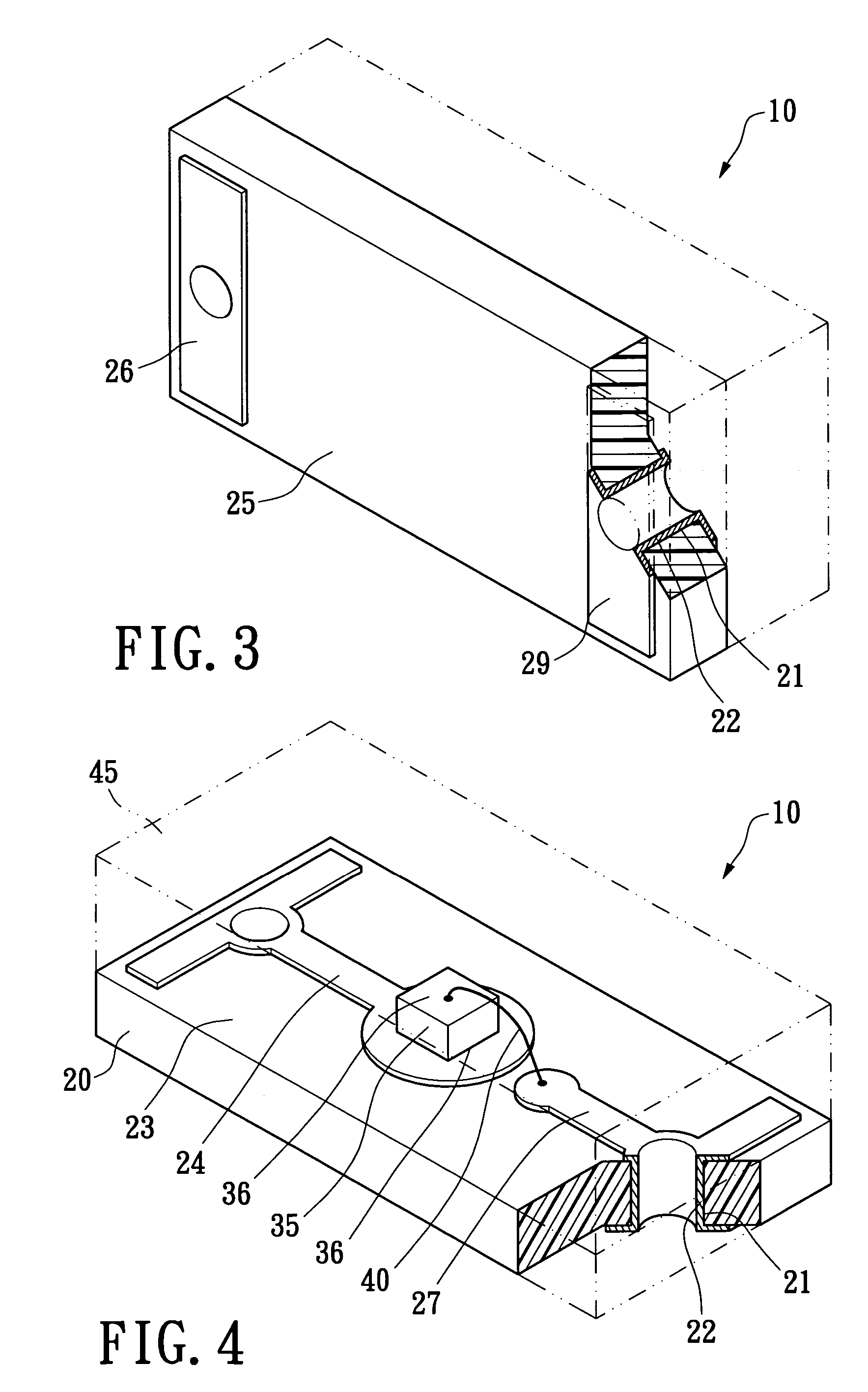
[0018]With reference to FIGS. 3 to 5, this invention is directed to an LED packaging structure 10, in which two holes 21 are formed on a substrate 20 thereof, and two conductors 22 extends along the pair of holes 21, respectively, such that one of the conductors 22 is connected to a conductive pad 24 on the upper surface 23 of the substrate 20 and a first electrode pad 26 on the lower surface 25 of the substrate 20, and the other conductor 22 is connected to a conductive strip 27 on the upper surface 23 of the substrate 20 and a second electrode pad 29 on the lower surface 25 of the substrate 20. Fabrication of the LED packaging structure 10 is thus easily performed and short-circuits between the adjacent LED packaging structures due to contact of conductive elements thereof can be avoided.

[0019]With reference to FIGS. 3 and 4, the substrate 20 has opposite upper and lower surfaces 23 and 25, and two holes 21 are formed through the upper and lower surfaces 23 and 25 on the substrate...


PUM


Abstract

An LED packaging structure has a substrate having two holes formed thereon. One of two conductive elements extends through the two holes to connect electrically to a conductive pad and a first electrode pad on the upper and lower surfaces of the substrate and the other of the two conductive elements extends through the holes to connect to the conductive strip and the second electrode pad on the upper and lower surfaces the substrate. A light-emitting chip electrically connects to the conductive pad and the conductive strip. The light-emitting chip is encapsulated by a protection colloid on the substrate, so as to make LED packaging structure easy to fabricate and avoid the short circuits of adjacent LED packaging structures due to contact between conductor materials therebetween.

Description

BACKGROUND OF THE INVENTION[0001]1. Field of the Invention[0002]The invention refers to a light-emitting diode (LED), and particularly to a packaging structure of an LED for improving fabricating yield and avoiding short circuit of adjacent LED packaging structures due to contact of their conductive elements.[0003]2. Description of the Prior Art[0004]Reference is made to FIG. 1, which is a prior art packaging structure of an LED as disclosed in U.S. Pat. No. Re. 36614, comprising a substrate 10a, a light-emitting chip 20a, a conducting wire 30a and a protective unit 40a (which is hereby incorporated by reference). The substrate 10a further comprises two conductor materials 50a respectively disposed on the upper surface of the substrate 10a to form a conductive pad 51a and a conductive strip 52a on the substrate 10a, respectively, and further extending respectively along the opposite half-circle side walls of the substrate 10a to the lower surface the substrate 10a to form an electro...

Claims


Application Information

Patent Timeline
Patent Type & Authority Patents(United States)
IPC IPC(8): H01L33/00H01L27/15H01L33/48H01L33/62H05K3/34
CPCH01L33/486H01L33/62H05K3/3442H01L2224/48091H01L2224/48227H01L2924/12041H05K2201/10636H05K2201/10666H05K2201/10106H01L2924/00014Y02P70/50
Inventor WANG, BILYCHUANG, JONNIELIN, CHUANFALEE, HENG-YEN
Owner HARVATEK CORPORATION
Why Eureka
Try Eureka