Probe sheet, probe card, semiconductor test equipment and semiconductor device fabrication method

a technology of probes and probes, which is applied in the direction of individual semiconductor device testing, semiconductor/solid-state device testing/measurement, instruments, etc., can solve the problems of complex fabrication process, difficulty in forming wires from contact terminals to wiring substrates, and inability to apply prior art to fine-pitch electrodes of semiconductor devices. , to achieve the effect of lowering the cost of the semiconductor device test process, reducing the whole fabrication cost, and increasing throughpu

Inactive Publication Date: 2006-05-23
RENESAS ELECTRONICS CORP
View PDF17 Cites 64 Cited by
  • Summary
  • Abstract
  • Description
  • Claims
  • Application Information

AI Technical Summary

Benefits of technology

[0010]It is another object of the present invention to provide a semiconductor device fabrication method that lowers the

Problems solved by technology

The prior art described in patent document 1 described above has the problem that, because the contact terminals have a mechanical structure (a spring probe having moving pins), this prior art cannot be applied to fine-pitch electrodes of a semiconductor device.
However, when many electrodes are tested, for example, when a plurality of semicondu

Method used


Image

  • Probe sheet, probe card, semiconductor test equipment and semiconductor device fabrication method
  • Probe sheet, probe card, semiconductor test equipment and semiconductor device fabrication method
  • Probe sheet, probe card, semiconductor test equipment and semiconductor device fabrication method

Examples


first embodiment

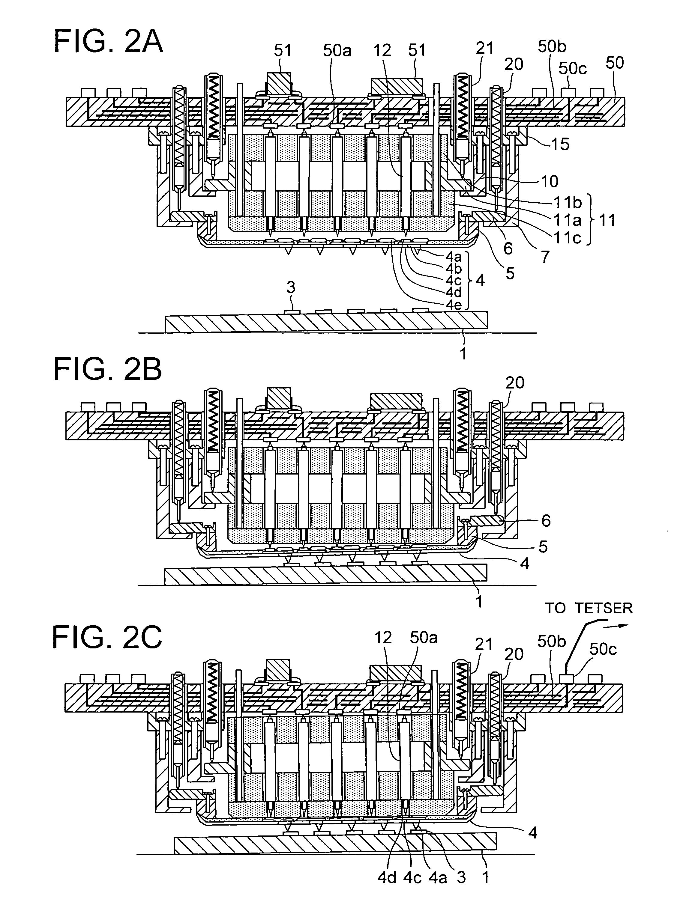
[0062]FIGS. 2A–2C show the major parts of a probe card in the present invention and show, in stages, the probing-time operation when there is a slight slant between the electrodes on the wafer and the contact terminals on the test equipment. FIG. 2A is a cross section diagram showing the status of the test equipment immediately before the probing operation, FIG. 2B is a cross section diagram showing the status of the test equipment that initially follows the slant of a wafer, and FIG. 2C is a cross section diagram showing the status of the test equipment that adds a desired load on the wafer surface to make an electrical characteristic test.

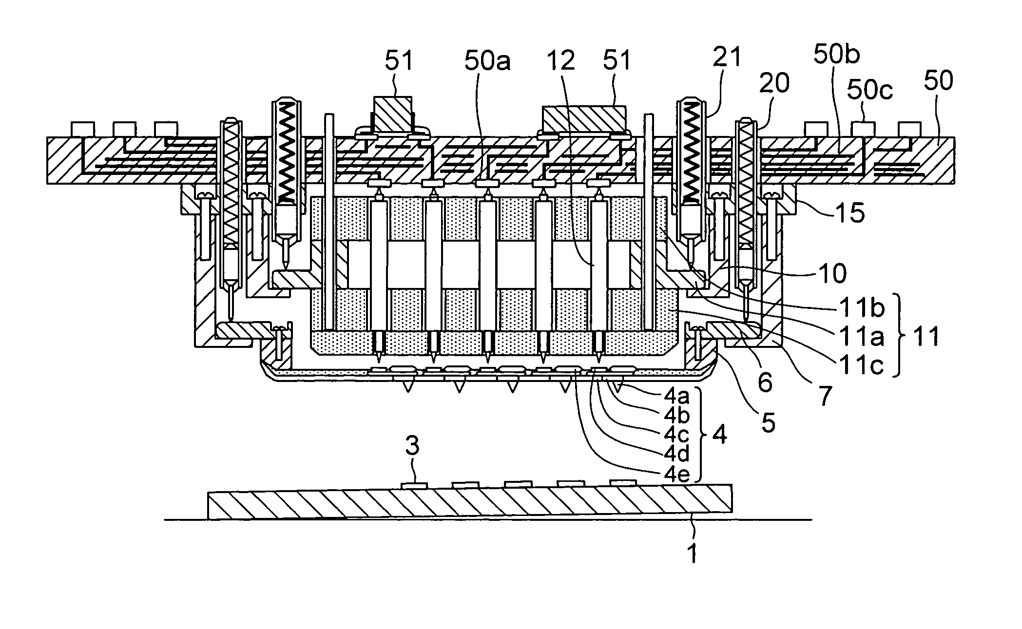
[0063]FIG. 2A shows the status of the test equipment immediately before the probing operation.

[0064]Spring probes 12 are inserted into a pressure member 11 composed of a pressure member holding substrate 11a held between a spring probe positioning upper substrate 11b and a spring probe positioning lower substrate 11c. One end of each spring probe...

third embodiment

[0078]FIG. 6 is a cross section diagram showing the major part of a probe card in the present invention. Bonding wires 55 are used for conduction from the lead-wire electrodes 4d on a probe sheet 4 to the electrodes 50a on a multi-layer wiring substrate 50. The bonding wire 55 is, for example, a gold wire or a gold wire coated with insulating materials. The moving action part of the probe card is constituted by a main spring (center pivot) 21a that fixes the probe sheet 4 onto a probe sheet holding substrate 6a through a probe sheet frame 5, that presses the probe sheet holding substrate 6a onto a temporary parallel motion support member (bottom) 7a fixed on the multi-layer wiring substrate 50 through a plurality of auxiliary springs 20, and that is positioned in the center of the probe sheet holding substrate 6a and fixed on the multi-layer wiring substrate 50. In this case, the tip of the main spring 21a is slightly spaced (about 0.05 mm) from the upper surface of the probe sheet ...

fifth embodiment

[0082]FIG. 8 is a cross section diagram showing the major part of a probe card in the present invention. A wire-drawing electrode 4d on a probe sheet 4 is connected to an electrode 50d on a multi-layer wiring substrate 50 as follows; one end of a bonding wire 55a is connected to the electrode 4d on the probe sheet 4 and the other end is connected to an electrode 62a on a wiring sheet 62, one end of a lead wire 60b is connected to an electrode 62c that is connected to the electrode 62a via an internal wire 62b on the wiring sheet 62, and the other end of the lead wire lead wire 60b is connected to the electrode 50d on the multi-layer wiring substrate 50 on which the wiring sheet 62 is fixed. This configuration allows the connection between the lead wire 60b and the electrode 50d on the multi-layer wiring substrate 50 to be changed and, in addition, the multi-layer wiring substrate 50 to be shared. The lead wire 60b may be a gold bonding wire, an enamel coated copper wire, or a coaxia...


PUM


Abstract

A probe card has first contact terminals electrically connected to the fine-pitch electrodes of a test target; wirings drawn from the first contact terminals; and second contact terminals electrically connected to the wirings, wherein the first contact terminals are formed each using an anisotropically etched hole in a crystalline substrate, and a semiconductor device test method (fabrication method) using the probe card.

Description

BACKGROUND OF THE INVENTION[0001]The present invention relates to a probe card, semiconductor test equipment, and a semiconductor device fabrication method.[0002]FIG. 21 shows an example of the flow of the semiconductor test process, which is one of semiconductor device fabrication processes performed after forming semiconductor device on a wafer. In the figure, packaging LSIs bear chips, and CSPs (Chip Scale Package) are shown as examples of semiconductor devices as a shipping form.[0003]Three main tests are made in the semiconductor device fabrication process as shown in FIG. 21. First, with semiconductor device circuits and electrodes formed on a wafer, a wafer test is made to check test the semiconductor device by open-short test and functional test. Next, a burn-in is made by testing semiconductor devices in a high-temperature or on high-voltage to find unstable semiconductor devices. Finally, a screening test is made to check the product performance before semiconductor device...

Claims


Application Information

Patent Timeline
IPC IPC(8): G01R31/02G01R1/067H01L21/66G01R1/073G01R3/00
CPCG01R1/0735G01R1/06744H01L24/05G01R1/06711H01L2224/73265G01R3/00G01R31/2874H01L2224/48465H01L2224/48091H01L2224/48227H01L2224/48247H01L2224/48453H01L2224/48463H01L2924/00014H01L2224/45144H01L2924/12042H01L2224/04042H01L2924/181H01L2224/32225H01L2224/32245H01L2924/15311H01L2924/14H01L2924/00011H01L2924/00H01L2924/00012H01L2924/01033H01L22/00
Inventor KASUKABE, SUSUMUHASEBE, TAKEHIKONARIZUKA, YASUNORIHASEBE, AKIO
Owner RENESAS ELECTRONICS CORP
Why Eureka
Try Eureka