Signal processing apparatus and method, and image sensing apparatus having a plurality of image sensing regions per image frame
- Summary
- Abstract
- Description
- Claims
- Application Information
AI Technical Summary
Benefits of technology
Problems solved by technology
Method used
Image
Examples
first embodiment
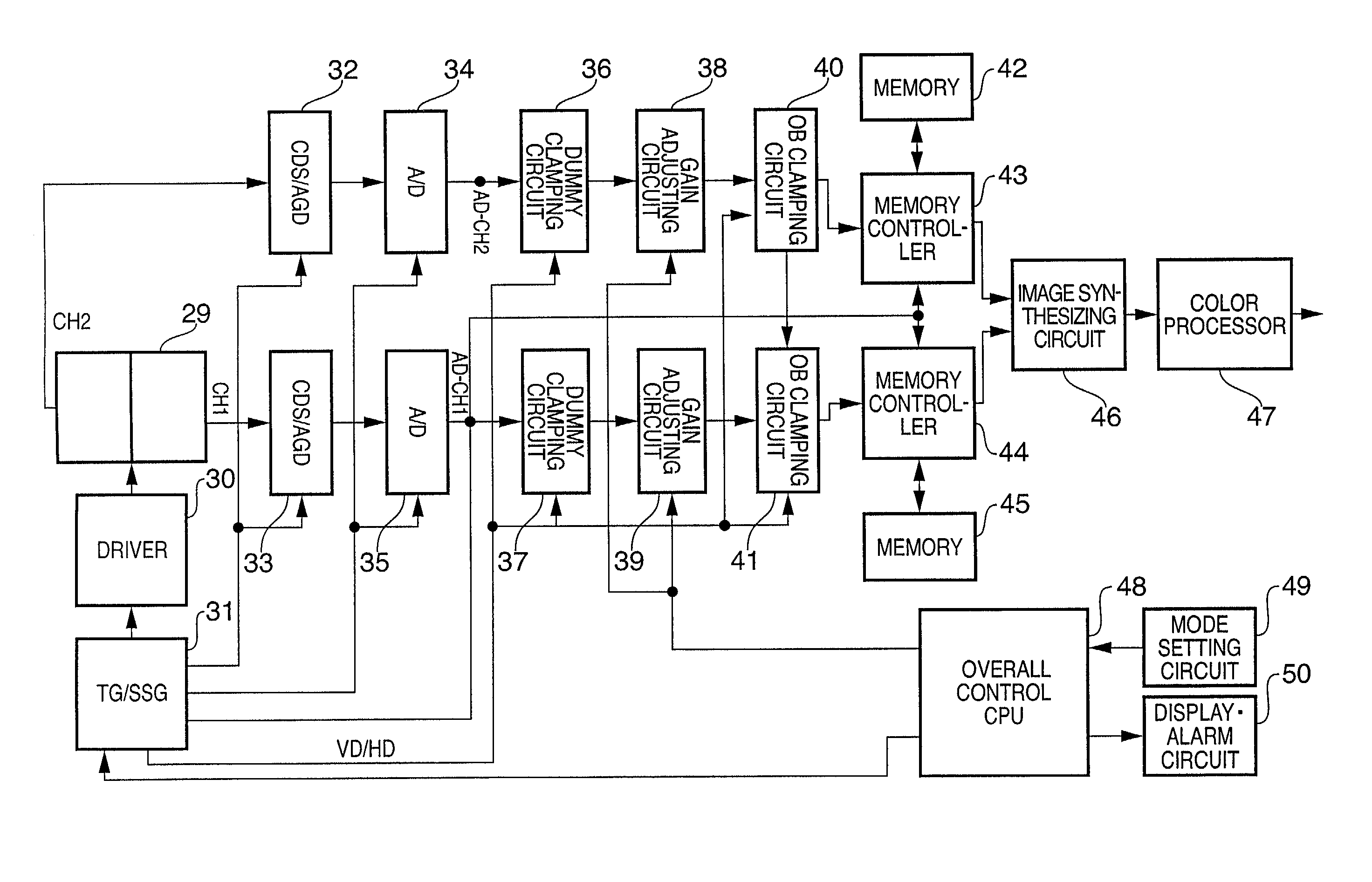
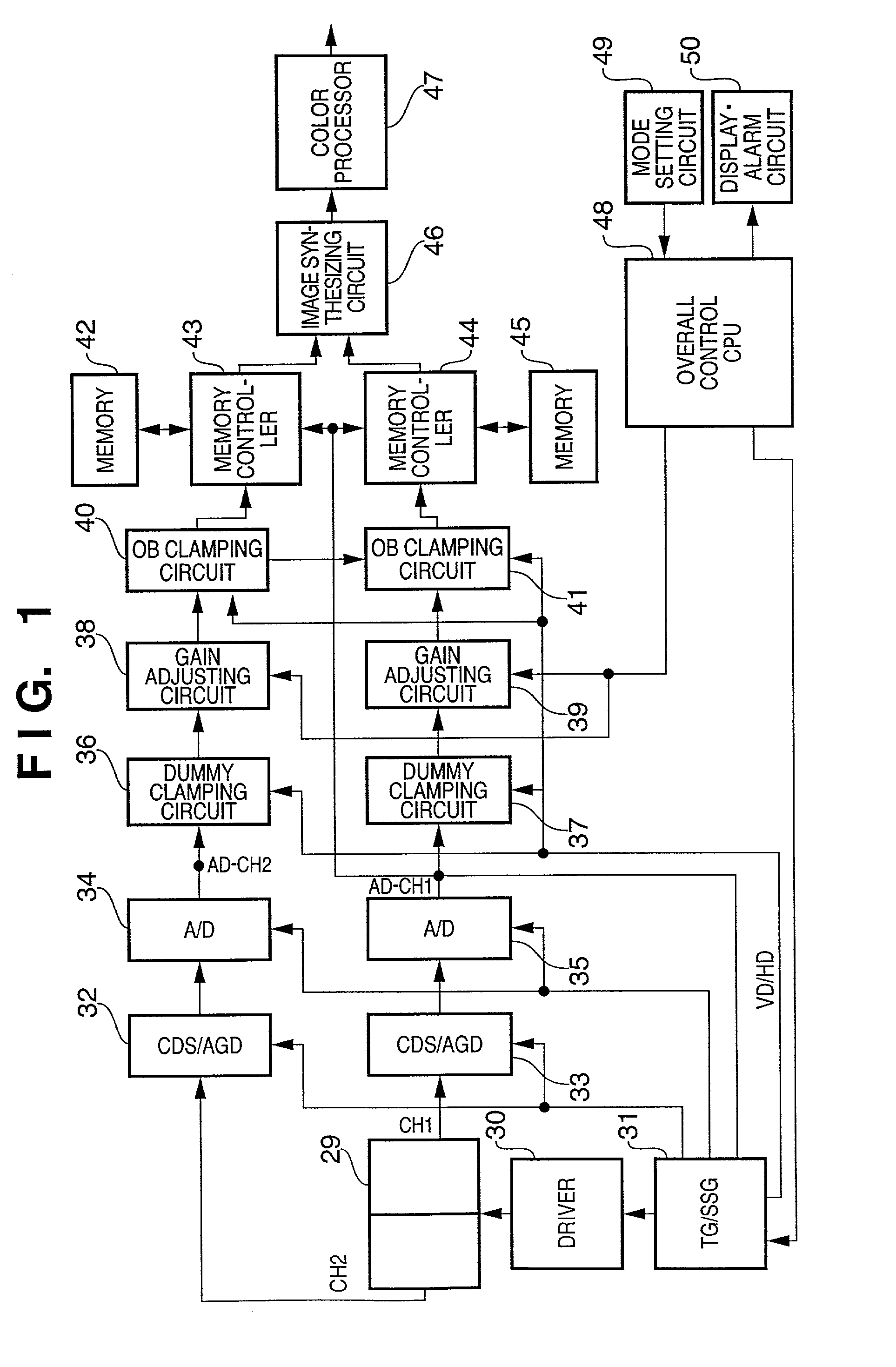
[0070]FIG. 1 is a block diagram schematically showing the hardware configuration of an image sensing apparatus (e.g., a digital camera) including a signal processing circuit according to a preferred embodiment of the present invention. In this embodiment, as an image sensing device for outputting image signals of a plurality of regions in parallel by dividing one frame into these regions, a CCD 29 which outputs image signals of two regions in parallel by dividing one frame into these two regions is used. This CCD 29 has two outputs (output terminals, output signals) CH1 and CH2 corresponding to the two regions. More specifically, the CCD 29 is driven by a driver 30 to operate at a predetermined frequency, and outputs left and right image signals separately by vertically dividing the whole frame as shown in FIG. 18.
[0071]An optical image of an object is formed on the image sensing surface of the CCD 29 by a main optical system (not shown). This optical image is photoelectrically conv...
second embodiment
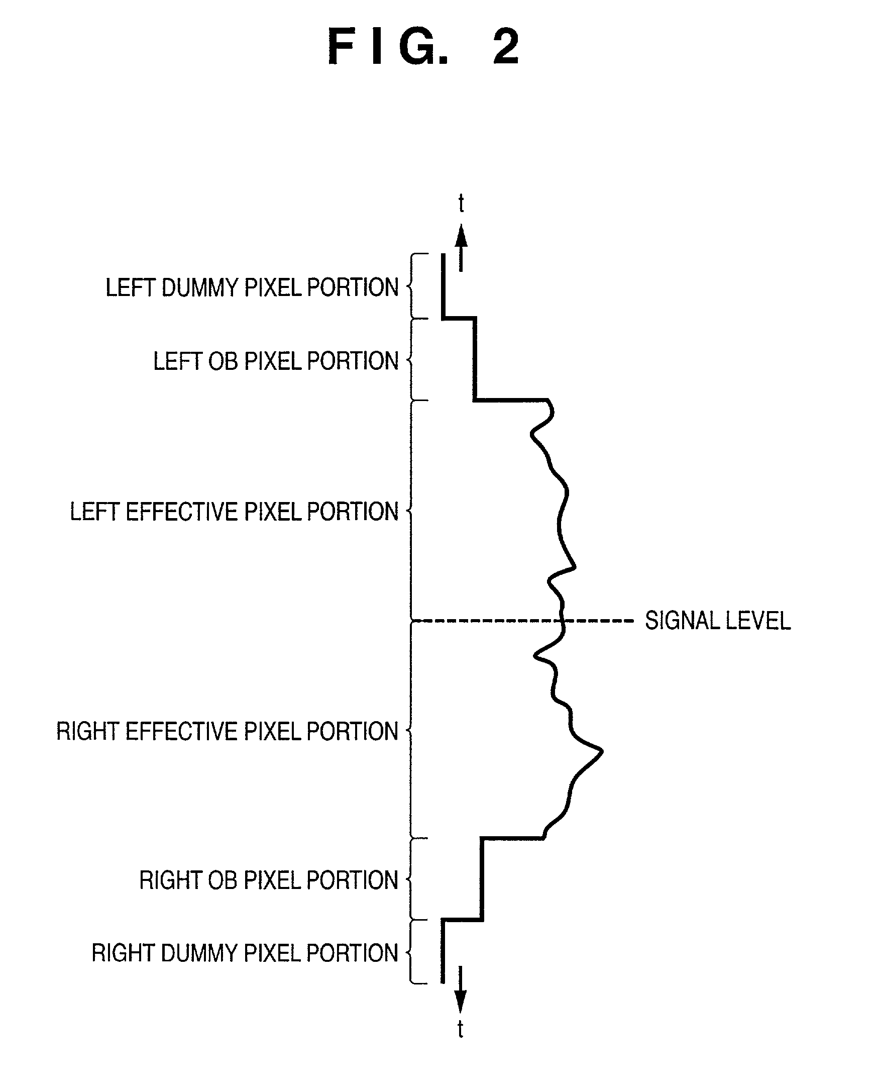
[0100]The second embodiment of the present invention will be described below. When an image sensing device 29 having a plurality of output terminals is a CCD as shown in FIG. 18 and HCCDs 57 and 58 keep transferring signals exceeding the number of stages of these HCCDs 57 and 58, as shown in FIG. 3, after charge signals of left and right dummy pixel portions, left and right OB pixel portions, and left and right effective pixel portions are output in this order, charge signals of left and right dummy pixel portions containing signal components of only the HCCDs 57 and 58 (i.e., not containing electric charge transferred from a VCCDs 60) are output. The left and right dummy pixel portions from which charge signals are output later will be called rear left and right dummy pixel portions. Further, the left and right dummy pixel portions output first will be called front left and right dummy pixel portions.
[0101]The charge signals output from the front left and right dummy pixel portions...
third embodiment
[0107]FIG. 4 is a schematic block diagram showing the arrangement of an image sensing apparatus such as a digital camera according to the third embodiment of the present invention.
[0108]As shown in FIG. 4, the image sensing apparatus includes an image sensing unit 101 such as a CCD area sensor, a microcomputer (PRS) 105 for controlling the overall image processing, an original image processor 110 for processing an image signal from the image sensing unit 101, an image processor 104 for receiving the output from the original image processor 110 and performing processing such as white balance correction and color interpolation, and a storage unit 103 having a nonvolatile storage device for saving image data of a plurality of images. The image sensing apparatus further includes a display processor 120 for displaying processed image data, a display memory 121, a display unit 122 such as an LCD, and a JPEG compressor 125 and storage device 130 for storing processed data.
[0109]The microco...
PUM
 Abstract
Description
Claims
Application Information


