
Optical receiver

a receiver and optical technology, applied in the field of optical receivers, can solve the problems of as little as possible and achieve the effect of avoiding high stray capacitance and impairing the sensitivity of the receiver

Inactive Publication Date: 2006-05-23
SCHOFIELD TECH
View PDF18 Cites 15 Cited by
  • Summary
  • Abstract
  • Description
  • Claims
  • Application Information

AI Technical Summary

Benefits of technology

[0014]It is an object of the invention to eliminate the drawbacks described above and to provide a solution wherewith the dynamic range of the receiver can be widened in such a way that the circuit solution will remain as simple as possible and furthermore in such a way that impairment in receiver sensitivity is minimal.
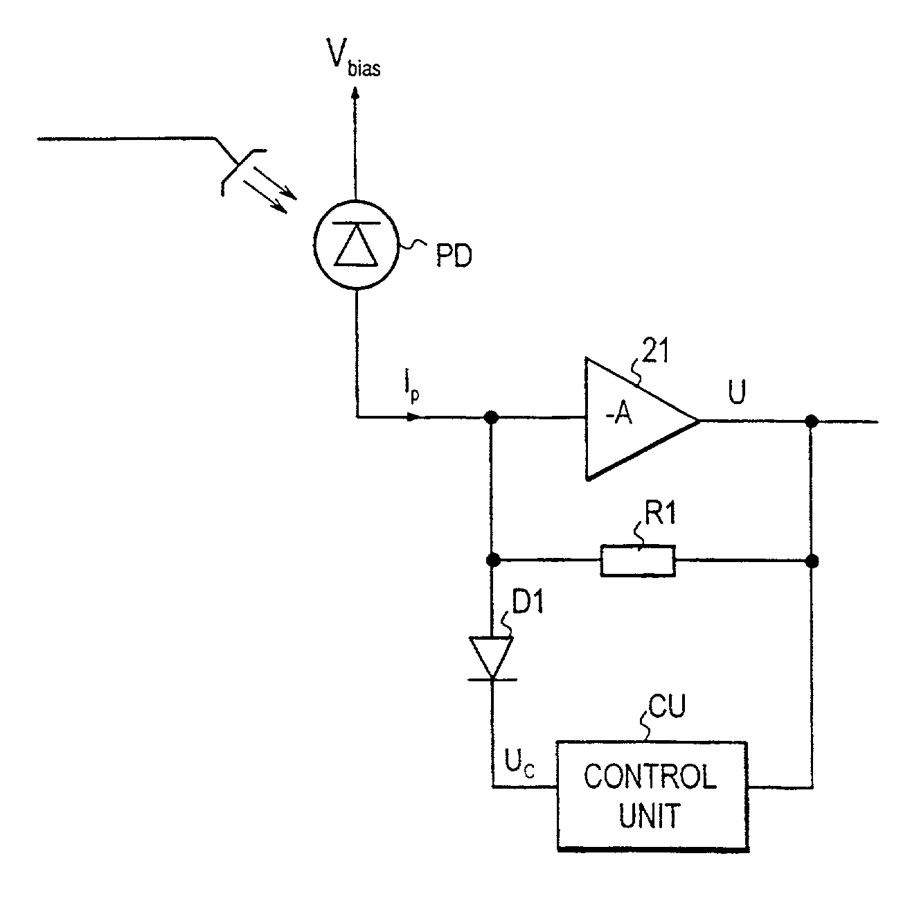
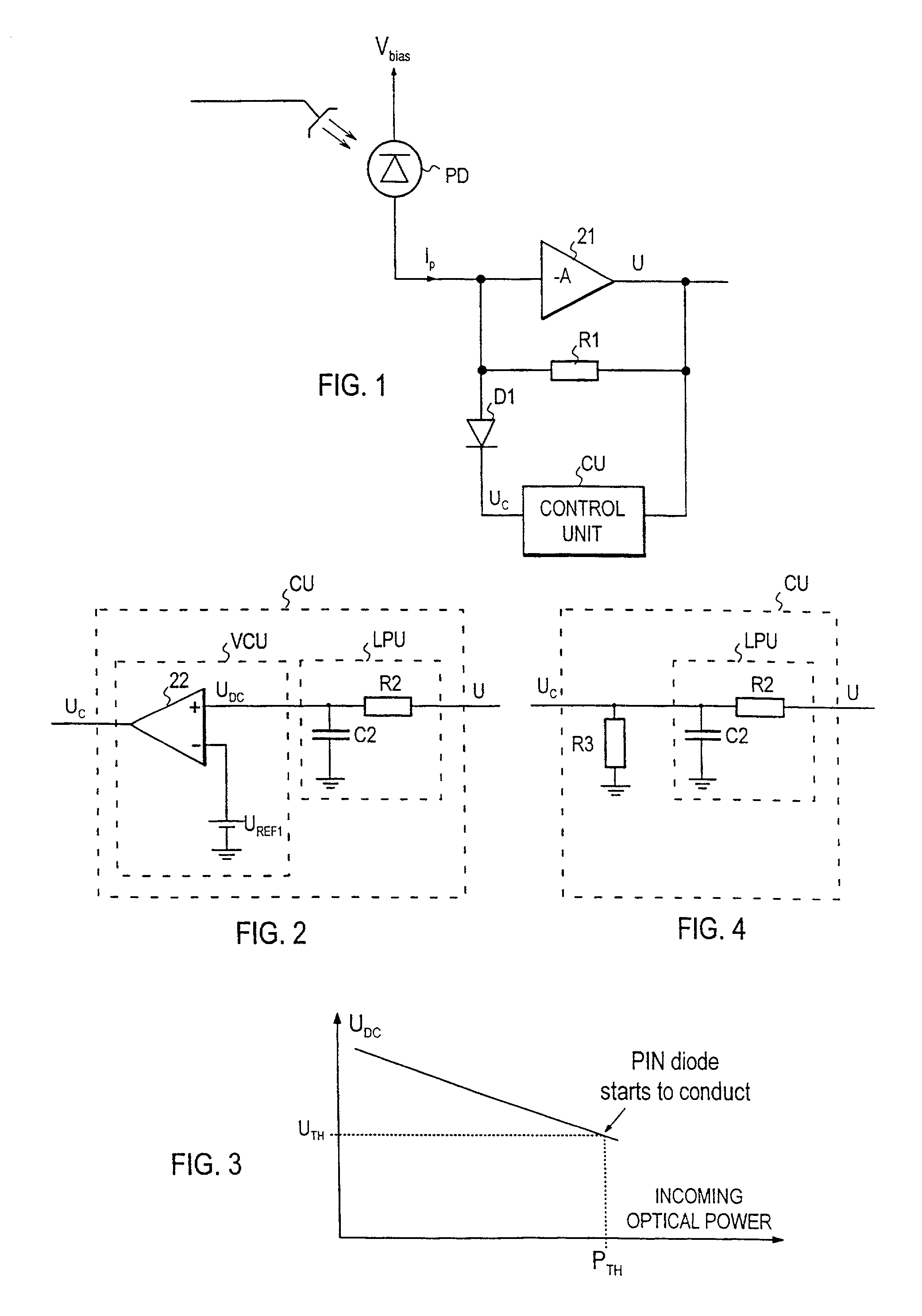
[0017]Since the PIN diode is in reverse when the adjustment is not operative and the adjustment requires no additional components on the input side of the transimpedance amplifier, no high stray capacitances are generated on the input side of the amplifier. Thus, by this means adding a control loop will impair the sensitivity of the receiver as little as possible.
[0018]An additional advantage of the solution in accordance with the invention is that conventional, inexpensive components can be used in the circuitry.

Problems solved by technology

Thus, by this means adding a control loop will impair the sensitivity of the receiver as little as possible.

Method used


Image

  • Optical receiver
  • Optical receiver

Examples


Embodiment Construction

[0024]As is known, a conventional non-optical PIN diode operates at low frequencies as a conventional diode (as a rectifier) but after a certain threshold frequency as a normal resistor. The dynamic resistance Rd of a PIN diode can, as is known, be represented by formula (1):

Rd=K / IDCX  (1)[0025]where IDC is the direct current passing through the diode and K and X are constants dependent on the properties of the diode and are indicated by the manufacturer of the diode.

[0026]In practice, a balanced line code (such as CMI or 5B6B) is used in optical transmission systems, and thus the received optical signal produces on the detector a current whose direct current component is half of the peak value Ipeak, i.e. IDC=0.5×Ipeak. When this current passes through the PIN diode, formula (2) is obtained for the peak value Upeak of the voltage over the PIN diode:

Upeak=Rd×Ipeak=K / IDCX×Ipeak=2×K×IDC1−X  (2)

[0027]However, with PIN diodes the constant X will typically have a value close to one, and ...


PUM


Abstract

The invention relates to an optical receiver comprising a transimpedance amplifier having an input and an output, a photo detector (PD) for converting the optical power arriving at the receiver, an adjustable impedance element (D1) operationally connected to the input of the transimpedance amplifier, and control means (CU) for controlling the current passinh through the impedance element by adjusting the impedance of the impedance means. In order for the receiver to have a high dynamic range, the adjustable impedance element is a PIN diode and the control means comprise (a) separating means (LPU) for separating the direct voltage component from the output voltage of the transimpedance amplifier, and (b) means (VCU) for adjusting the voltage over the PIN diode directly on the basis of the separated direct voltage component.

Description

[0001]This application is a continuation of international application serial number PCT / FI98 / 00891, filed 13 Nov. 1998.FIELD OF THE INVENTION[0002]The invention relates generally to an optical receiver. More specifically, the invention relates to a control loop to be used in an optical receiver, wherewith the dynamic range of the input amplifier is widened.BACKGROUND OF THE INVENTION[0003]An optical transmission system comprises an optical transmitter converting an electrical signal to be transmitted into optical form, (b) an optical fibre serving as a conductor for the optical signal, and (c) an optical receiver detecting the transmitted optical signal and converting it into electrical form.[0004]A typical optical receiver comprises at its input stage a photo detector and a transimpedance amplifier whose input is connected to the photo detector. The photo detector converts the optical signal it has received into electric current that is supplied to the transimpedance amplifier. The...

Claims


Application Information

Patent Timeline
Patent Type & Authority Patents(United States)
IPC IPC(8): H04B10/06H03F1/08H03F3/08H04B10/69
CPCH03F1/08H04B10/6931H03F3/087
Inventor RANTAKARI, ERKKI
Owner SCHOFIELD TECH
Learn More