Stable electroless fine pitch interconnect plating

a technology of electroless fine pitch and interconnects, which is applied in the direction of individual semiconductor device testing, semiconductor/solid-state device testing/measurement, instruments, etc., can solve the problems of reducing yield, poor solderability of die contacts, and difficult to plate conductive metals onto very fine pitch features, etc., to achieve stable plating bath and facilitate the plating of small contact features

Inactive Publication Date: 2006-05-30
MICRON TECH INC
View PDF7 Cites 9 Cited by
  • Summary
  • Abstract
  • Description
  • Claims
  • Application Information

AI Technical Summary

Benefits of technology

[0004]The invention further provides a method of plating die contacts of a plurality of dice (chips) on a wafer, which includes fabricating the larger supplemental plating structures on the wafer, fabricating a conductive connection between the supplemental plating structures and the die contacts, maintaining a plating bath, inserting the wafer into the plating bath, and plating the supplemental plating structures and die contacts. Plating of the die contacts is induced as a result of the conductive connection to the supplemental plating structures. The method and apparatus facilitate the plating of a small contact feature of a wafer die while providing a relatively stable plating bath.

Problems solved by technology

As integrated circuit devices become increasingly complex and feature sizes become increasingly smaller, it becomes more difficult to plate conductive metals onto the very fine pitch features.
Improper or incomplete plating of the bond pads results in die contacts having poor solderability, which decreases yield.
Also, it can be difficult to maintain the stability of baths in which parts of various sizes are plated.

Method used


Image

  • Stable electroless fine pitch interconnect plating
  • Stable electroless fine pitch interconnect plating
  • Stable electroless fine pitch interconnect plating

Examples


Embodiment Construction

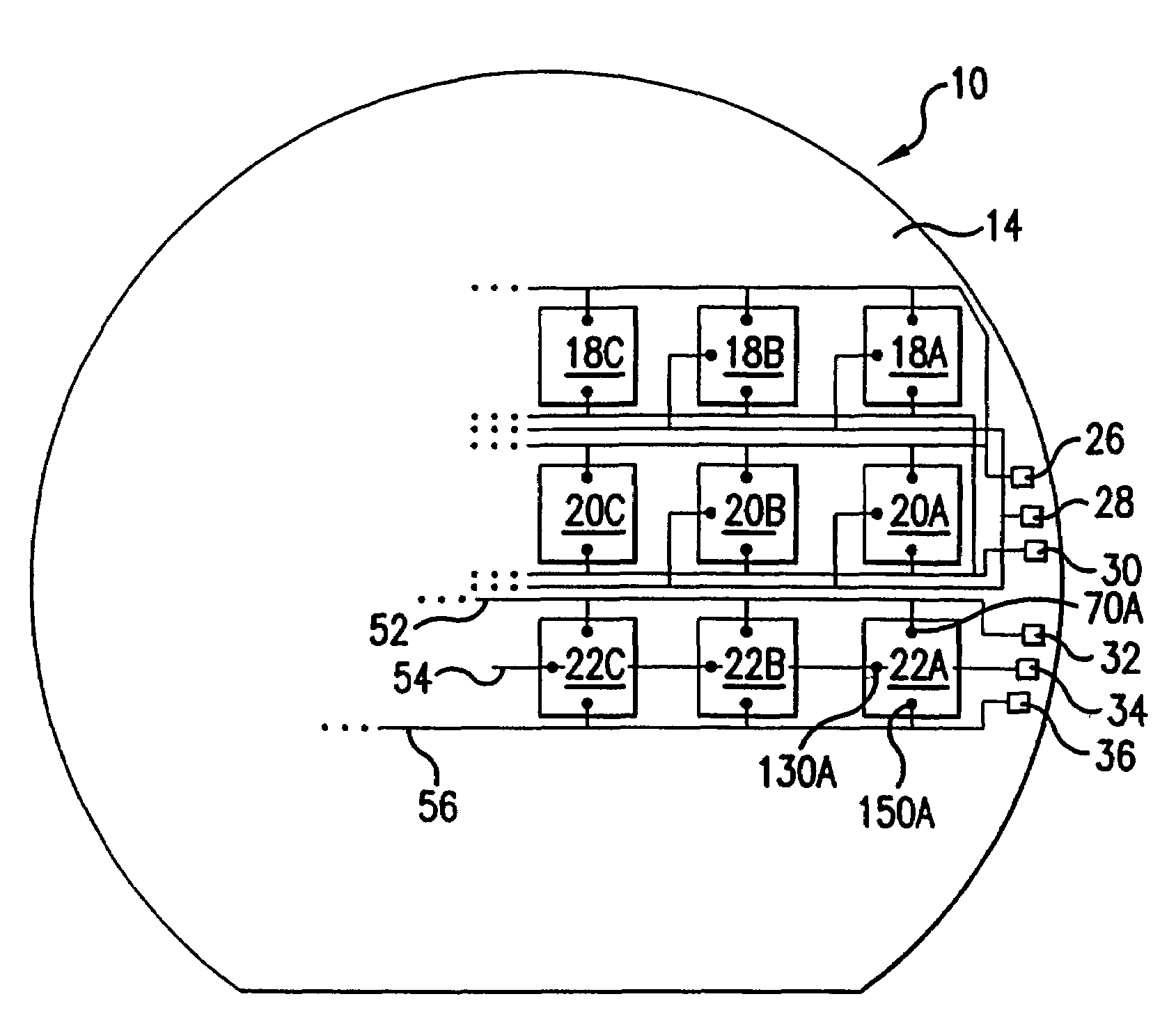
[0012]Referring to FIG. 1, a semiconductor wafer 10 fabricated in accordance with an exemplary embodiment of the invention includes a substrate 14 on which numerous dice are formed through etching, deposition, and other integrated circuit (IC) fabrication techniques. The substrate 14 may be formed of a variety of semiconductor materials known in the art including silicon and gallium-arsenide, among others. The wafer 10 is not limited to any particular size or shape.

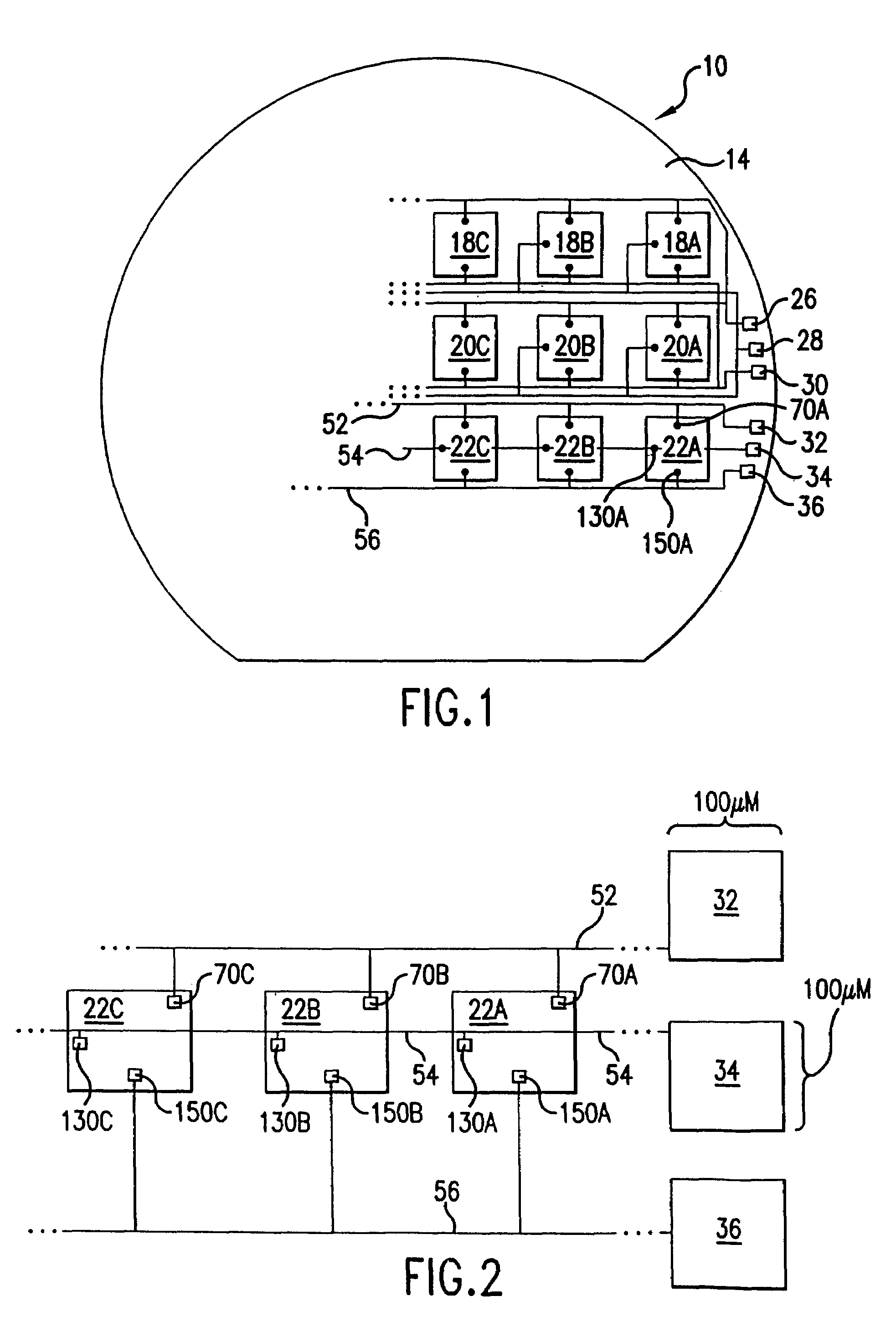
[0013]Each wafer 10 includes many dice. For clarity of illustration, only dice 18A–C, 20A–C, and 22A–C (collectively “dice 18–22”) are shown in FIG. 1. The dice are fabricated in the aggregate on wafer 10, and after fabrication are singulated from wafer 10 using a cutting process, for example. The separation takes place along the areas between adjacent dice, the so-called “street” areas.

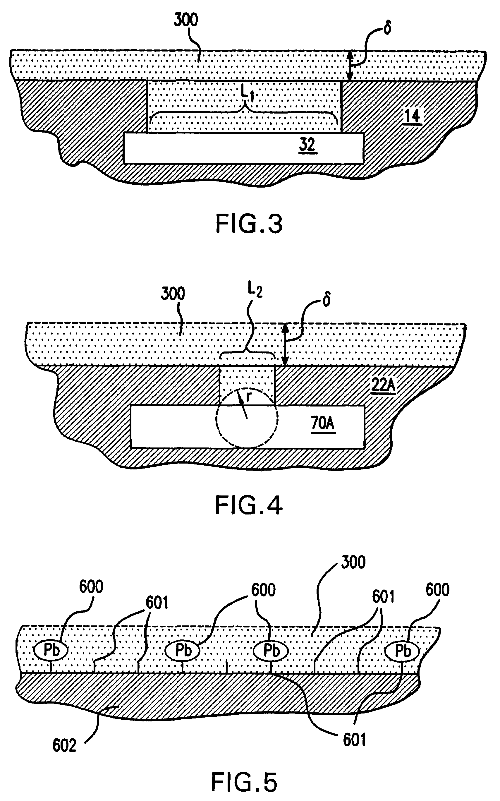
[0014]FIG. 2 shows a portion of the die 22 in greater detail. Small bond pads, e.g., 70A, 130A, 150A, are provided on each die. The bond ...


PUM


Abstract

A method and apparatus for plating facilitates the plating of a small contact feature of a wafer die while providing a relatively stable plating bath. The method utilizes a supplemental plating structure that is larger than a die contact that is to be plated. The supplemental plating structure may be located on the wafer, and is conductively connected to the die contact. Conductive connection between the die contact and the supplemental plating structure facilitates the plating of the die contact. The supplemental plating structure also can be used to probe test the die prior to singulation.

Description

FIELD OF THE INVENTION[0001]The invention relates to apparatus and techniques for plating small surface features of an integrated circuit device.BACKGROUND OF THE INVENTION[0002]As integrated circuit devices become increasingly complex and feature sizes become increasingly smaller, it becomes more difficult to plate conductive metals onto the very fine pitch features. For example, bond pads formed on dies require plating to form die contacts. Improper or incomplete plating of the bond pads results in die contacts having poor solderability, which decreases yield. Also, it can be difficult to maintain the stability of baths in which parts of various sizes are plated. Consequently, a system for plating small die features, using a stable plating bath, is desired.BRIEF SUMMARY OF THE INVENTION[0003]The present invention provides an integrated circuit plating apparatus having a bath for plating die contacts on wafers. Prior to plating, die contacts are conductively connected to larger sup...

Claims


Application Information

Patent Timeline
Patent Type & Authority Patents(United States)
IPC IPC(8): H01L21/66H01L21/288H01L21/44H01L23/485
CPCH01L21/288H01L24/02H01L2924/01033H01L2924/01006H01L2924/01011H01L2924/01014H01L2924/01016H01L2924/01028H01L2924/01046H01L2924/0105H01L2924/01051H01L2924/01052H01L2924/01078H01L2924/01082H01L2924/014H01L2924/14
Inventor LINDGREN, JOSEPH T.
Owner MICRON TECH INC
Why Eureka
Try Eureka