Method of manufacturing electrical parts

a manufacturing method and technology of electrical parts, applied in the field of manufacturing electrical parts, can solve the problems of high contact resistance of the surface thereof, and achieve the effect of reducing the contact resistance on the surface of the electrical parts and good plating

Inactive Publication Date: 2006-03-02
SUMITOMO ELECTRIC IND LTD
View PDF4 Cites 8 Cited by
  • Summary
  • Abstract
  • Description
  • Claims
  • Application Information

AI Technical Summary

Benefits of technology

[0015] With the manufacturing method of electrical parts according to the present invention, since no metal fluoride film is formed on the surface of the metal layer by removing the metal oxide film generated as a result of polishing the metal layer, a good plating can be formed on the surfaces of the electrical parts, whereby contact resistance on the surfaces of the electrical parts can be decreased.

Problems solved by technology

Then, the metal layer is partly removed by polishing the portion excessively deposited due to electroforming.
However, regarding an electrical part made by such a method as described above, there was the problem that the contact resistance of the surface thereof was high.

Method used


Image

  • Method of manufacturing electrical parts
  • Method of manufacturing electrical parts
  • Method of manufacturing electrical parts

Examples


embodiment 1

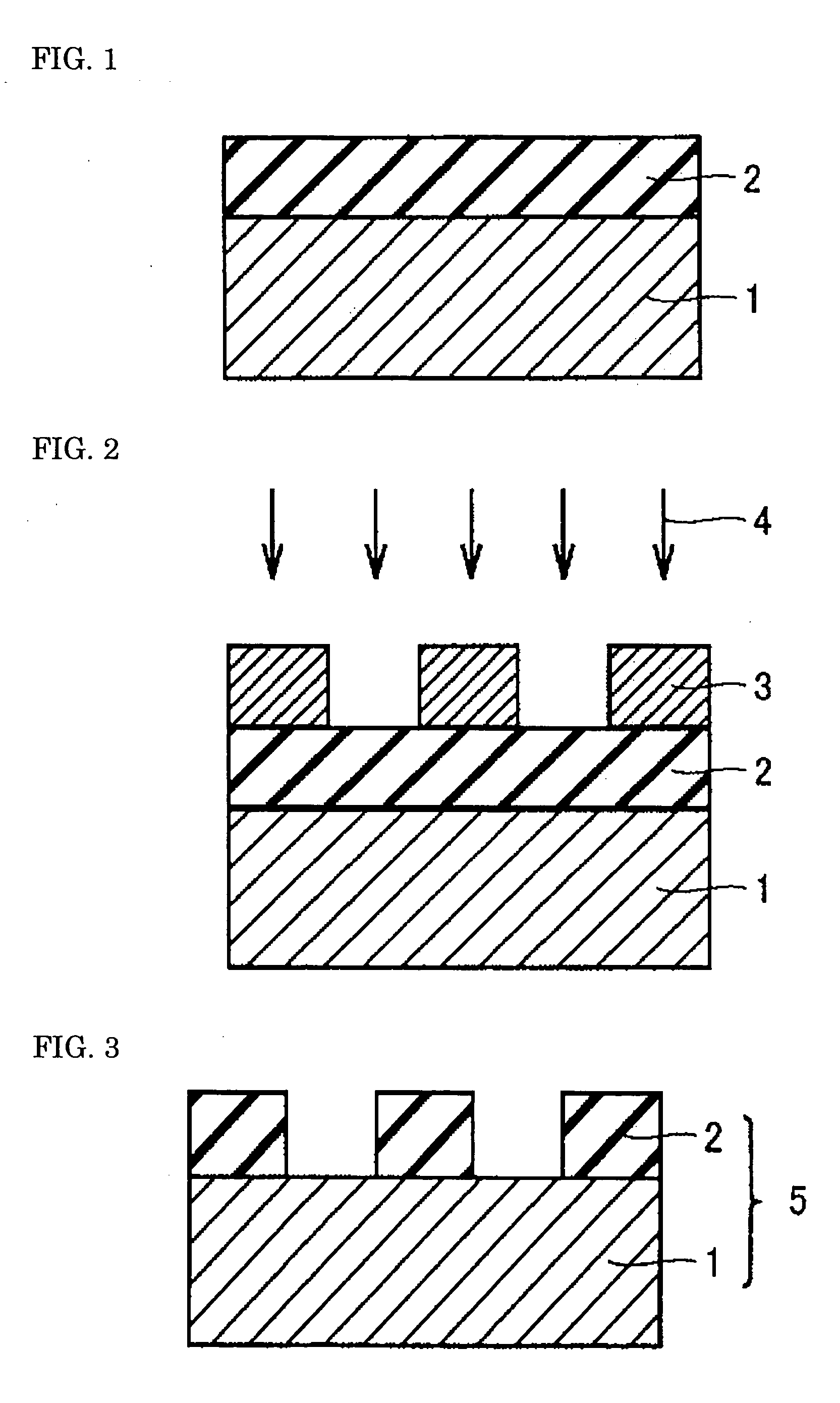
[0030] A preferable example of the manufacturing method of electrical parts according to the present invention will be described in reference to the drawings. First, as schematically shown in the sectional view of FIG. 1, a photoresist 2 is applied to the whole surface of a conductive substrate 1. In this case, the substrate 1 may be an electroconductive substrate made of stainless steel, copper or aluminum, etc. or may be a substrate in which a conductive layer is formed by sputtering titanium, aluminum, copper, or alloy of these metals on a non-electroconductive substrate made of silicon or glass, etc. As for the photoresist, a resin such as polymethyl methacrylate (PMMA), which includes carbon and hydrogen, is used, for example.

[0031] Subsequently, as shown in the schematic sectional view of FIG. 2, after a mask 3 in which openings are formed in a desired pattern is placed on the surface of the photoresist 2, X-rays 4 are irradiated from a position above the mask 3. Then, as sho...

embodiment 2

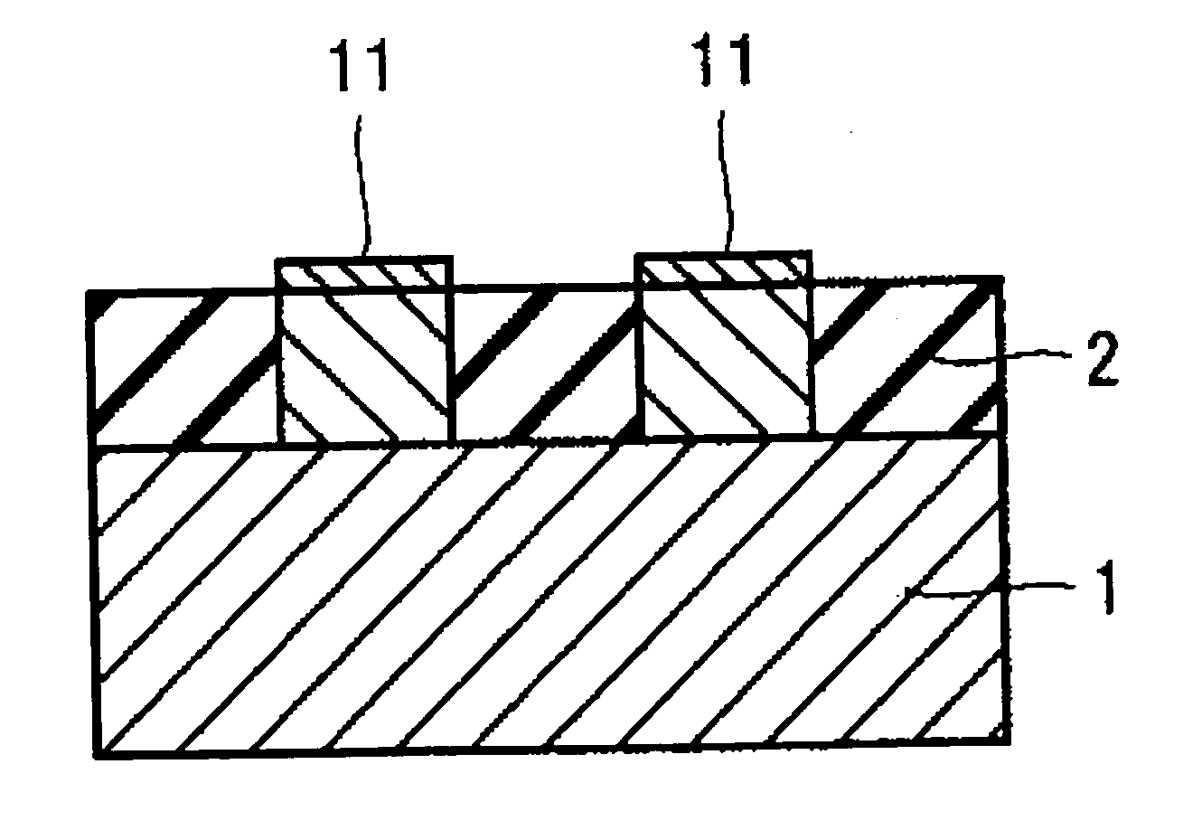
[0038] In reference to the drawings, another preferable example of the manufacturing method of electrical parts according to the present invention will be described hereinafter. First, as shown in the schematic sectional view of FIG. 10, the steps of manufacture until the step of removing the metal oxide film formed on the surface of the metal layer 6 are the same as in the above-described embodiment 1. Next, as shown in the schematic sectional view of FIG. 11, oxidation prevention members 11 are provided on the surfaces of the metal layers 6. The oxidation prevention member 11 is not particularly limited if it can prevent the oxidation of the surface of the metal layer 6: it may be formed by electroplating with a metal such as copper, for example.

[0039] As shown in the schematic sectional view of FIG. 12, the photoresist 2 on the substrate 1 is removed by performing ashing by means of plasma using a gas which includes oxygen and fluorine compound such as carbon tetrafluoride or xe...

example 1

[0041] A photoresist consisting of PMMA was applied onto the whole surface of a substrate made of stainless steel, and after irradiating synchrotron radiation (SR), which is X-ray, to a part of the photoresist, the irradiated part of the photoresist was removed to expose the surface of the substrate so that the photoresist having openings with the removed parts of 60 μm width, 1 mm length and 60 μm depth was formed.

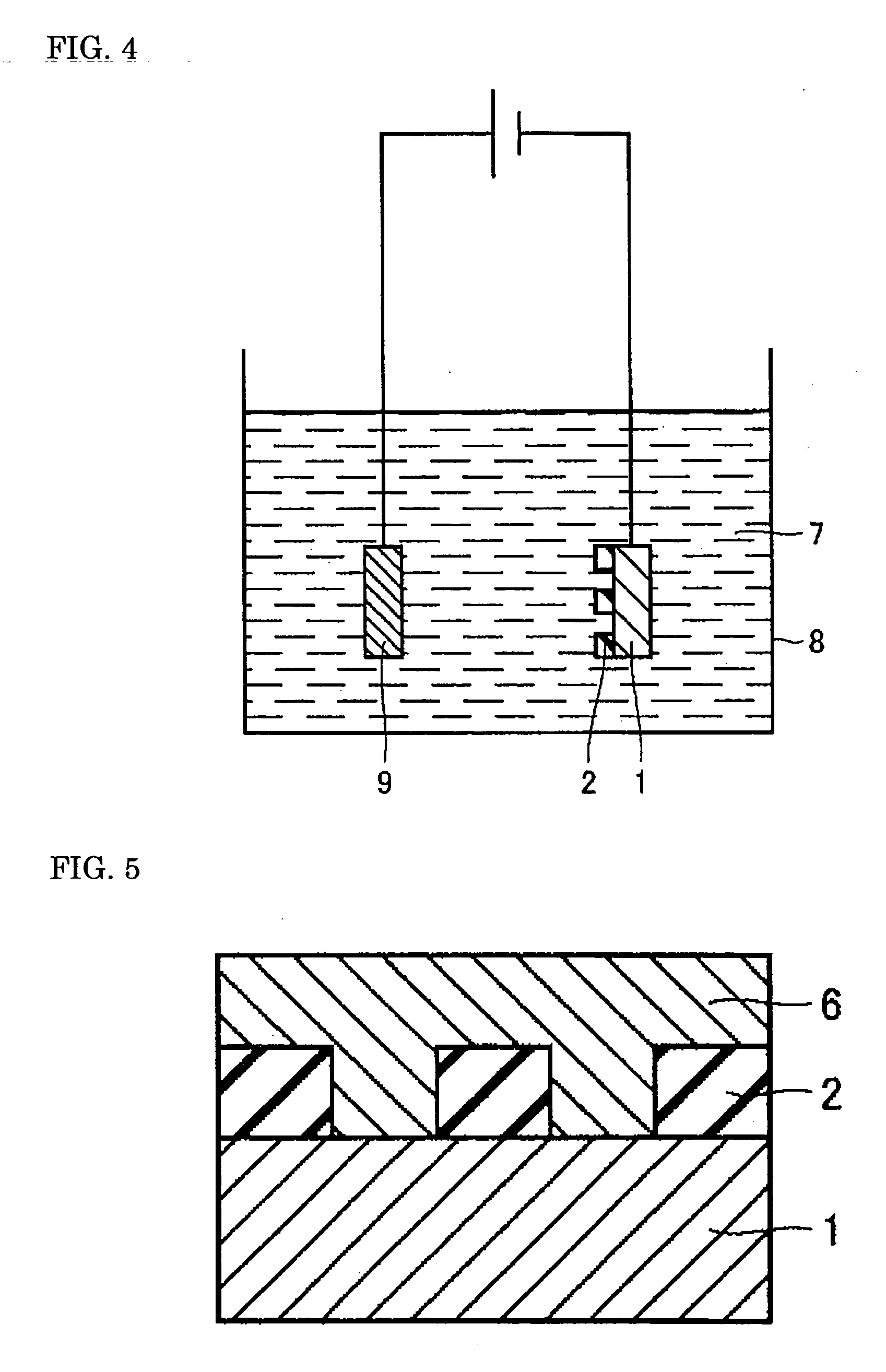
[0042] The master die thus prepared was used as a cathode and a nickel board was used as an anode such that these electrodes were put in an electrolysis solution of pH 4.0 having the following composition and contained in an electroplating bath. Thus, electroforming was performed while the electrolysis solution was maintained at a temperature of 60° C. and an electric current with an electric current density of 4A / dm2 was caused to flow between these electrodes. The notation of the compositions of the electrolysis solution described below represents the mass or volume of...


PUM

PropertyMeasurementUnit
depthaaaaaaaaaa
widthaaaaaaaaaa
widthaaaaaaaaaa

Abstract

A method of manufacturing electrical parts is provided, which method comprises the steps of: forming a photoresist on a part of the surface of a substrate; forming a metal layer on the surface of the substrate after the photoresist has been formed; removing a part of the metal layer; removing a metal oxide film formed on the: surface of the metal layer as a result of removing a part of the metal layer; and removing the photoresist. With this method the contact resistance on the surfaces of the electrical parts can be decreased.

Description

BACKGROUND OF THE INVENTION [0001] 1. Field of the Invention [0002] The present invention relates to methods of manufacturing electrical parts, and particularly to manufacturing methods with which contact resistance on the surface of an electrical part can be decreased. [0003] 2. Description of the Background Art [0004] In the past, lithography using ultraviolet irradiation was used for making fine electrical parts consisting of metals such as Ni (nickel) and Ni alloy with electroforming. However, in recent years, increasing need of electrical parts having higher precision and higher aspect ratio has attracted attention to the so-called LIGA (Lithographie Galvanoformung Abformung) process, in which lithography, plating such as electroforming, and molding are combined. It is possible to make electrical parts having sizes of micron order by the LIGA process, particularly by X-ray lithography using synchrotron radiation (SR). [0005] An example of the methods of manufacturing electrical...

Claims


Application Information

Patent Timeline
Patent Type & Authority Applications(United States)
IPC IPC(8): H01L21/44
CPCB81B2201/018B81B2207/07B81C1/00698C25D5/022H05K2203/1157C25D5/34H05K3/205H05K2203/0315C25D5/10H01L21/288
Inventor NITTA, KOJIINAZAWA, SHINJIHIRATA, YOSHIHIROOKADA, KAZUNORI
Owner SUMITOMO ELECTRIC IND LTD
Why Eureka
Try Eureka