Sealed pores in low-k material damascene conductive structures

a technology of damascene and conductive structures, which is applied in the manufacturing of semiconductor/solid-state devices, basic electric elements, electric apparatus, etc., can solve the problems of increasing the complexity of the manufacturing process, increasing the functional complexity of the integrated circuit, and challenging various aspects of multi-level interconnect processes, so as to improve the reliability of semiconductor devices, prevent device failures, and increase device yield

Inactive Publication Date: 2006-05-30
INFINEON TECH AG
View PDF13 Cites 34 Cited by
  • Summary
  • Abstract
  • Description
  • Claims
  • Application Information

AI Technical Summary

Benefits of technology

[0022]These and other problems are generally solved or circumvented, and technical advantages are generally achieved, by preferred embodiments of the present invention, which provide a method and structure for lining the inner surface of pores of porous low-dielectric constant materials on sidewalls of patterned damascene structures, preventing copper migration.
[0025]Advantages of preferred embodiments of the present invention include providing a method of sealing sidewalls and surfaces of damascene structures with an oxide, wherein the inner surfaces of the pores of a porous low-dielectric constant material are fully lined to prevent copper migration into the low-dielectric constant material. Reliability of semiconductor devices is improved, and device yields are increased. Device failures are also prevented.

Problems solved by technology

Scaling or reducing the size increases circuit performance, primarily by increasing circuit speed, and also increases the functional complexity of the integrated circuits.
Implementing a multilevel interconnect process to a fabrication scheme increases the complexity of the manufacturing process.
As semiconductor devices continue to shrink, various aspects of multilevel interconnect processes are being challenged.
The propagation delay of integrated circuits becomes limited by the large RC time delay of interconnection lines when minimum feature size is decreased below about 1 μm, for example.
The change in both the conductive materials and insulating materials used in multilevel interconnect schemes is proving challenging and requires a change in a number of processing parameters.
However, the RC (resistance / capacitance) time delay of copper conductive lines can be problematic, so low-dielectric constant materials are used to reduce the capacitive coupling and reduce the RC time delay between interconnect lines.
However, copper easily migrates into low-dielectric constant materials, which can cause shorting and create device failures.
The copper diffusion channel that is created within porous low-dielectric constant materials 122 and 106 causes reliability problems in semiconductor devices 100, causing shorts and devise failures.

Method used


Image

  • Sealed pores in low-k material damascene conductive structures
  • Sealed pores in low-k material damascene conductive structures
  • Sealed pores in low-k material damascene conductive structures

Examples


Embodiment Construction

[0033]The making and using of the presently preferred embodiments are discussed in detail below. It should be appreciated, however, that the present invention provides many applicable inventive concepts that can be embodied in a wide variety of specific contexts. The specific embodiments discussed are merely illustrative of specific ways to make and use the invention, and do not limit the scope of the invention.

[0034]The present invention will be described with respect to preferred embodiments in a specific context, namely a semiconductor device and the BEOL of the fabrication process. The invention may also be applied to conductive layers formed in an FEOL, for example.

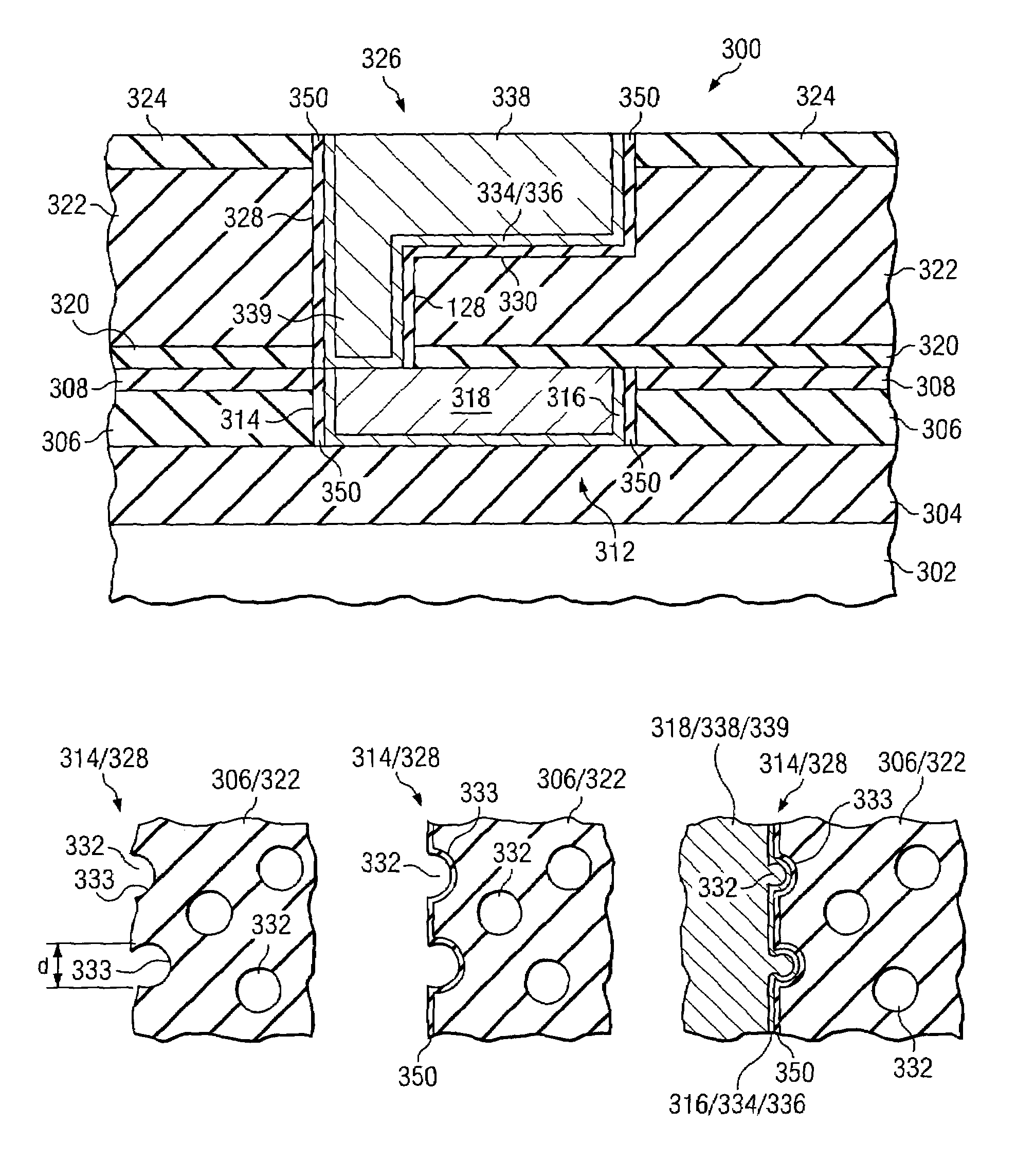
[0035]With reference now to FIG. 3A, therein is shown a cross-sectional view of a semiconductor device 300 having a multi-level interconnect structure formed in accordance with a preferred embodiment of the present invention. A workpiece 302 is provided. The workpiece 302 may include a semiconductor substrate compris...


PUM

PropertyMeasurementUnit
diameteraaaaaaaaaa
diameteraaaaaaaaaa
dielectric constantaaaaaaaaaa

Abstract

An oxide layer is used to seal pores in porous low-dielectric constant materials, thus preventing the migration of subsequently deposited copper materials into the porous low-dielectric constant materials in damascene processes. The oxide layer is deposited over the inner surface of at least one pore along a sidewall of the patterned low-dielectric constant material. In one embodiment, the oxide layer is deposited using atomic layer deposition (ALD), and the oxide layer comprises SiO2.

Description

TECHNICAL FIELD[0001]The present invention relates generally to semiconductor devices, and more particularly to a method and device for preventing copper migration into damascene-patterned porous low-dielectric constant material layers of a semiconductor device.BACKGROUND[0002]In the evolution of integrated circuits in semiconductor technology, there has been a trend towards device scaling. Scaling or reducing the size increases circuit performance, primarily by increasing circuit speed, and also increases the functional complexity of the integrated circuits. The number of devices per chip has increased throughout the years. When integrated circuits contained only a small number of devices per chip, the devices could be easily interconnected in a single level. However, the need to accommodate more devices and increased circuit speed has led to the use of multi-level or multi-layer interconnects.[0003]In a multi-level interconnection system, the area needed by the interconnect lines ...

Claims


Application Information

Patent Timeline
Patent Type & Authority Patents(United States)
IPC IPC(8): H01L21/4763H01L21/768
CPCH01L21/76831H01L21/76807
Inventor KIM, SUN-OO
Owner INFINEON TECH AG
Why Eureka
Try Eureka