Ceramic package with radiating lid

a ceramic package and lid technology, applied in the direction of semiconductor devices, semiconductor/solid-state device details, electrical apparatus, etc., can solve the problems of increasing the failure rate of wire bonding, the radiation of chip-type devices, and the difficulty of mounting the saw duplexer b>

Inactive Publication Date: 2006-05-30
SAMSUNG ELECTRO MECHANICS CO LTD
View PDF9 Cites 30 Cited by
  • Summary
  • Abstract
  • Description
  • Claims
  • Application Information

AI Technical Summary

Benefits of technology

[0010]Accordingly, the present invention has been made keeping in mind the above problems occurring in the prior art, and an object of the present invention is to provide a ceramic package with a lid covering on the top surface of a package substrate, which is intended to radiate heat generated during an operation of a chip-type device such as an SAW filter, by improving the configuration of the lid to allow the heat to be radiated therefrom, instead of the formation of additional via holes for transferring heat.

Problems solved by technology

Since such heat gives birth to noise or malfunction of the device, various structures for radiating heat are in demand.
Due to the miniaturization of packages, there is a problem in heat radiation of chip-type devices such as SAW filters.
In the manufacture of the package substrate, since the electrodes 110 are embedded in the bottom of the package substrate on which the SAW duplexer 102 is mounted, roughness is caused by deterioration of the bottom surface, thereby causing difficulty in mounting of the SAW duplexer 100.
In addition, because of the uneveness of the bottom surface, the upper surface of the SAW duplexer 102 is not level at the time of wire bonding process, thereby increasing the failure rate of wire bonding.
This results in a camber phenomenon of the package.
However, since the phase control circuit 108 must be formed in a substrate to be separated from the via holes 110, there is a limitation in its design.

Method used


Image

  • Ceramic package with radiating lid
  • Ceramic package with radiating lid
  • Ceramic package with radiating lid

Examples


Embodiment Construction

[0023]This invention will be described in further detail by way of example with reference to the accompanying drawings.

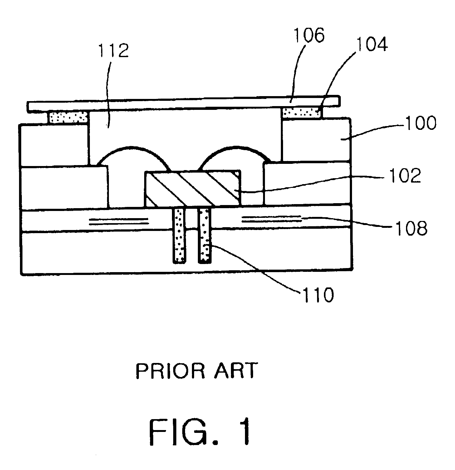
[0024]The ceramic package with a radiating lid according to the present invention is characterized in that a substrate having a chip-type device mounted thereon is not formed with via holes, and the lid for closing a cavity of a package substrate is modified, unlike a conventional ceramic package.

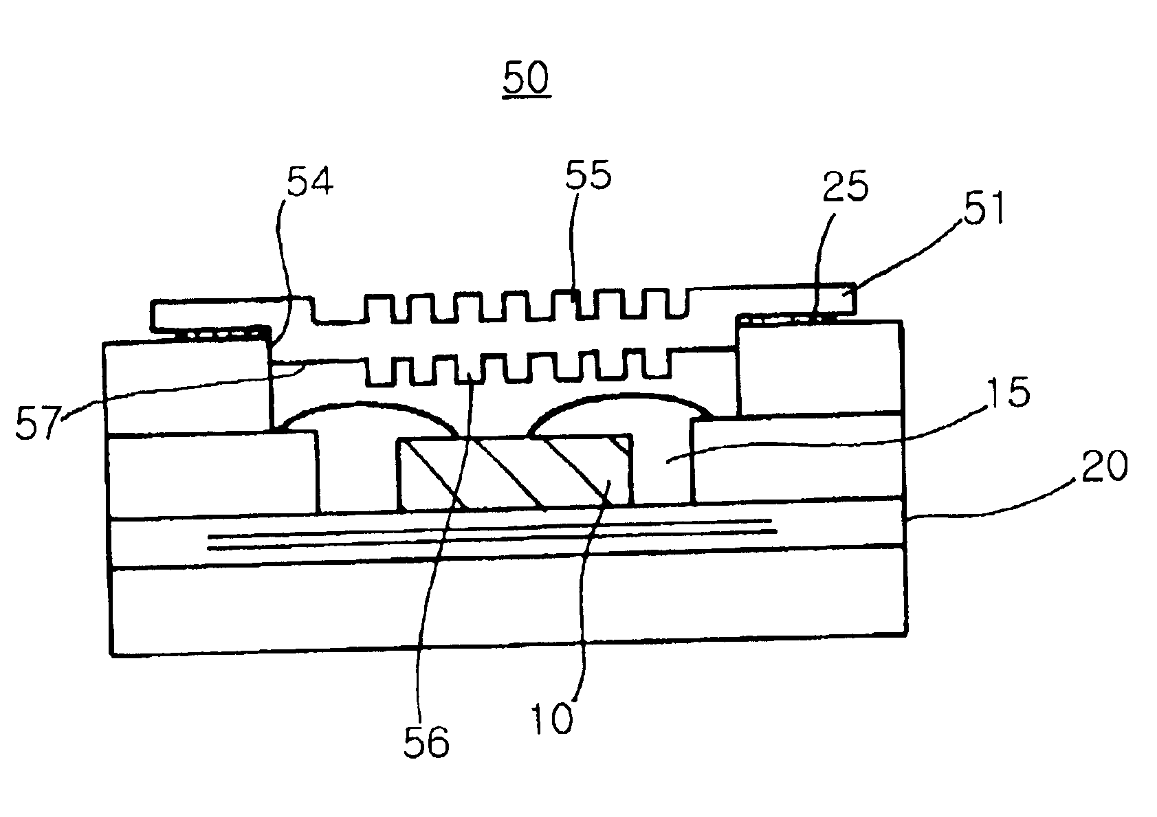
[0025]FIG. 3 is a cross-sectional view of a ceramic package with an improved lid according to the present invention. As shown in the drawing, a ceramic package 30 includes a chip-type device 10 mounted in a cavity 15 internally formed in a laminated substrate 20. The chip-type device 10 is a kind of heating element such as a semiconductor, an SAW filter and a quartz oscillator, and is described focusing on the SAW filter in the following embodiments. The laminated substrate is made of ceramic excellent in thermal conductivity and is comprised of the bottom substrate and sub...


PUM

PropertyMeasurementUnit
dimensionsaaaaaaaaaa
roughnessaaaaaaaaaa
impedanceaaaaaaaaaa

Abstract

A ceramic package with a lid attached thereon, which has radiating grooves at its upper surface and/or lower surface to radiate heat generated from a chip-type device is disclosed. The ceramic package includes a laminated ceramic substrate comprised of a plurality of ceramic substrate such that a cavity is centrally defined in the laminated ceramic substrate, a chip-type device mounted on the bottom of the cavity of the laminated ceramic substrate, and a lid attached to the top of the laminated ceramic substrate to close the cavity, which is provided at its upper and/or lower surface with protrusions to efficiently radiate heat generated from the chip-type device.

Description

BACKGROUND OF THE INVENTION[0001]1. Field of the Invention[0002]The present invention relates to a ceramic package with a lid for radiating and eliminating unwanted heat generated from a chip-type device during an operation of the device, and more particularly to a ceramic package with a lid covering the ceramic package, which is provided at its upper surface with radiating grooves or pins to allow heat generated from the chip-type device to be efficiently radiated to the outside.[0003]2. Description of the Prior Art[0004]In general, a chip-type device mounted on a product is sure to generate heat during its operation. Since such heat gives birth to noise or malfunction of the device, various structures for radiating heat are in demand.[0005]In particular, in order to manufacture simple and light mobile phones, surface acoustic wave filters (referred to as “SAW filters” hereinafter) and surface acoustic wave duplexers (referred to as “SAW duplexers” hereinafter) have become more and...

Claims


Application Information

Patent Timeline
Patent Type & Authority Patents(United States)
IPC IPC(8): H01L23/12H01L23/02H01L23/367
CPCH01L23/3675H01L2924/3011H01L2224/48091H01L2224/48227H01L2924/00014H01L23/367
Inventor CHO, SEONG WON
Owner SAMSUNG ELECTRO MECHANICS CO LTD
Why Eureka
Try Eureka