Lateral heat spreading layers for epi-side up ridge waveguide semiconductor lasers

a semiconductor laser and heat dissipation layer technology, applied in the direction of lasers, semiconductor lasers, basic electric elements, etc., can solve the problems of reducing affecting the performance of the device, so as to reduce the thermal resistance of the semiconductor device

Inactive Publication Date: 2006-06-13
ARMY US SEC THE
View PDF10 Cites 55 Cited by
  • Summary
  • Abstract
  • Description
  • Claims
  • Application Information

AI Technical Summary

Benefits of technology

[0020]In view of the foregoing, an embodiment of the invention provides a semiconductor device comprising a substrate, a mesa region adjacent the substrate, an electroplated (or otherwise-deposited) metal layer surrounding the mesa region, and an insulator layer separating a side portion of the mesa region from the electroplated metal layer, wherein the electroplated metal layer is dimensioned and configured to have a thickness of at least half a thickness of the mesa region; and to laterally spread heat away from the mesa region. Moreover, the mesa region (or semiconductor region) comprises a first cladding layer adjacent to the substrate, an active region adjacent to the first cladding layer, and a second cladding layer adjacen...

Problems solved by technology

However, the epi-side down process is more complicated and has a significantly lower yield than the epi-side up process.
Despite the huge variety of commercially available SDLs emitting in the near-IR spectral region (λ
Until recently, there se...

Method used


Image

  • Lateral heat spreading layers for epi-side up ridge waveguide semiconductor lasers
  • Lateral heat spreading layers for epi-side up ridge waveguide semiconductor lasers
  • Lateral heat spreading layers for epi-side up ridge waveguide semiconductor lasers

Examples


Embodiment Construction

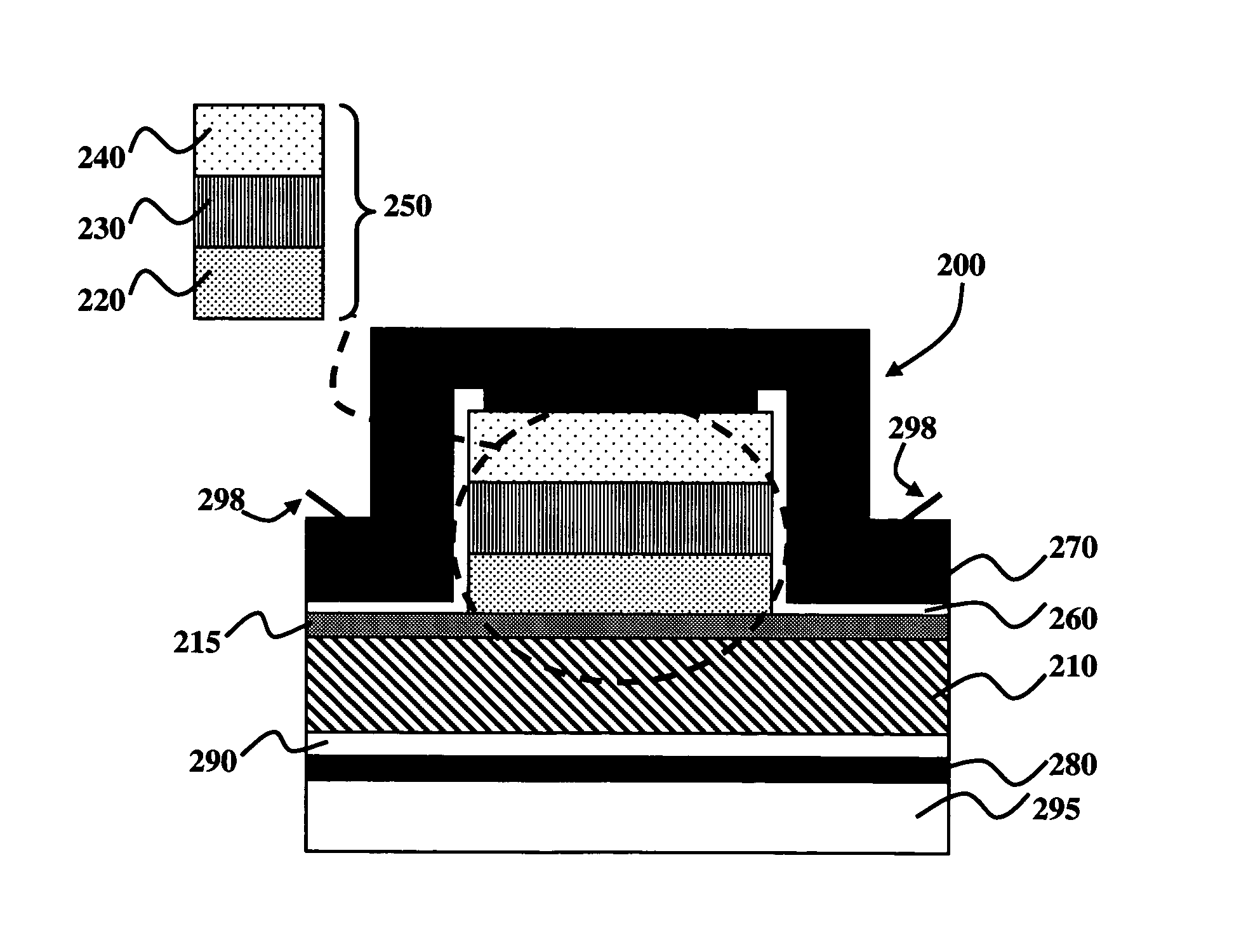
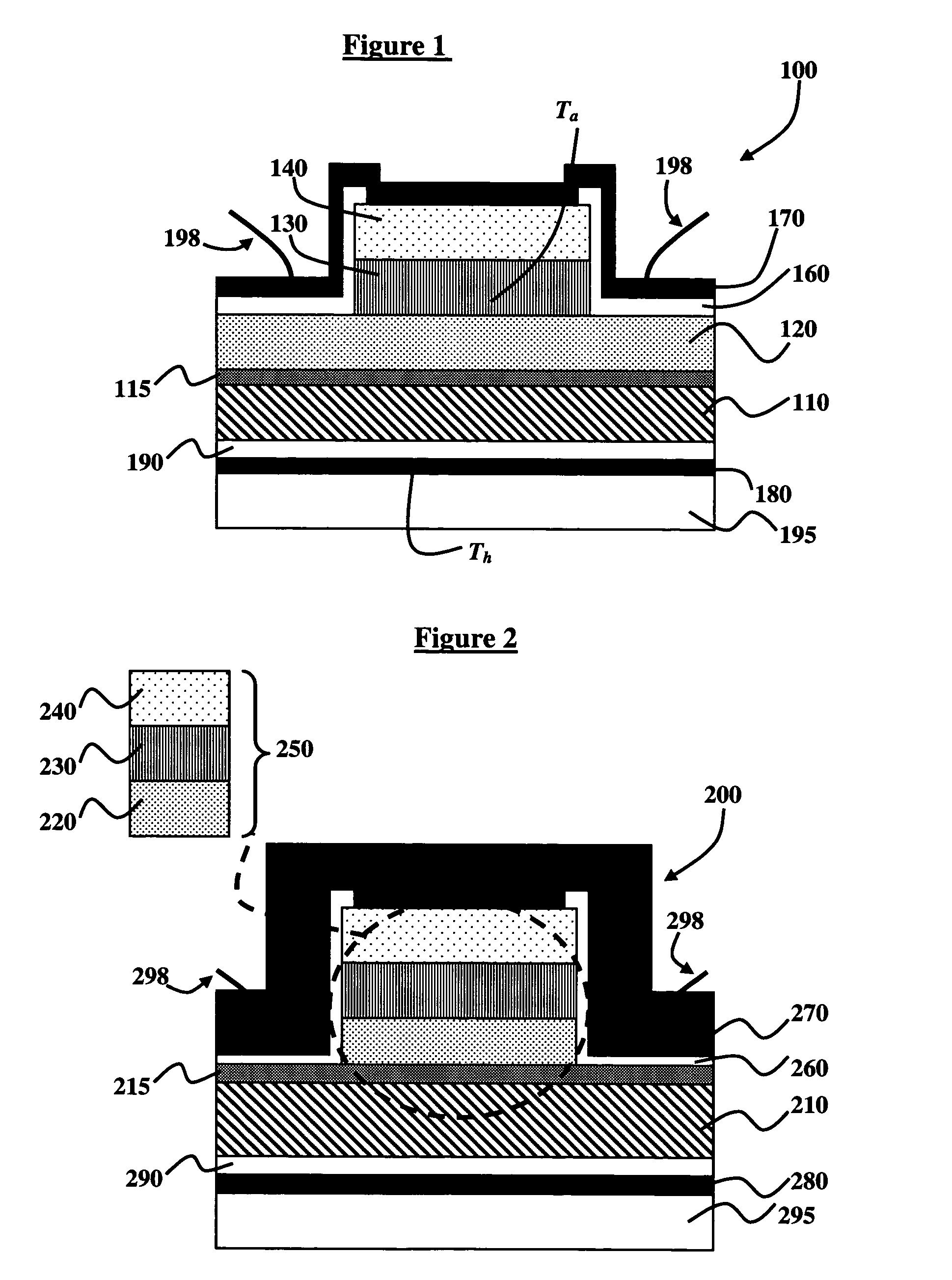
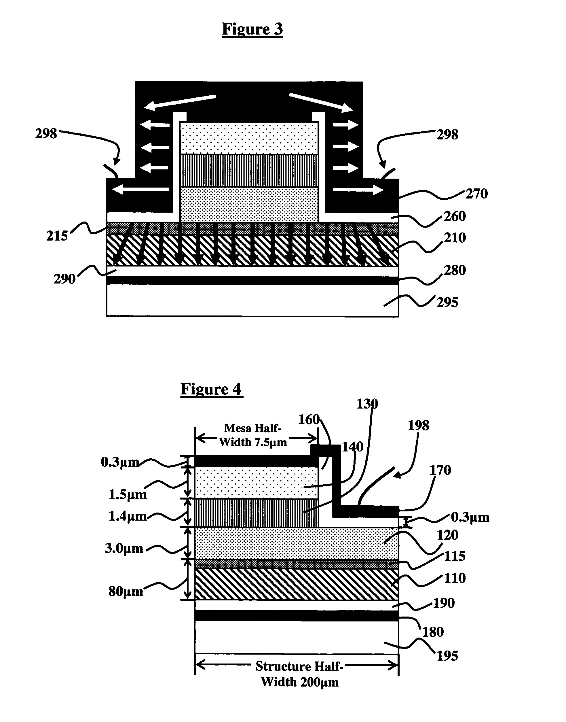
[0035]The invention and the various features and advantageous details thereof are explained more fully with reference to the non-limiting embodiments that are illustrated in the accompanying drawings and detailed in the following description. It should be noted that the features illustrated in the drawings are not necessarily drawn to scale. Descriptions of well-known components and processing techniques are omitted so as to not unnecessarily obscure the invention. The examples used herein are intended merely to facilitate an understanding of ways in which the invention may be practiced and to further enable those of skill in the art to practice the invention. Accordingly, the examples should not be construed as limiting the scope of the invention.

[0036]As previously mentioned, there is a need for a new and improved semiconductor device to decrease the thermal resistance of IC lasers mounted in a conventional epi-side-up configuration. The invention provides a semiconductor device 2...


PUM


Abstract

Disclosed are a semiconductor device and method of manufacturing the same comprising a substrate, a mesa region adjacent to the substrate, an electroplated metal layer, for reducing the thermal resistance of the device, surrounding the mesa region, an insulator layer separating a side portion of the mesa region from the electroplated metal layer, a heat sink, a bonding layer adjacent to the heat sink, and a second metal layer in between the substrate and the heat sink, wherein the substrate is adjacent to the bonding layer, and wherein the electroplated metal layer dimensioned and configured to have a thickness of at least half a thickness of the mesa region; and to laterally spread heat away from the mesa region. The mesa region comprises a first cladding layer adjacent to the substrate, an active region adjacent the first cladding layer, and a second cladding layer adjacent to the active region.

Description

CROSS-REFERENCE TO RELATED APPLICATION[0001]This application claims the benefit of U.S. Provisional Patent Application No. 60 / 499,064 filed Aug. 26, 2003, the complete disclosure of which is herein incorporated by reference.GOVERNMENT INTEREST[0002]The invention described herein may be manufactured, used, and / or licensed by or for the United States Government.BACKGROUND OF THE INVENTION[0003]1. Field of the Invention[0004]The invention generally relates to heat dissipation layers for semiconductor devices, and more particularly to a semiconductor device with a metal layer above and beyond the region confined by the optical mode of a semiconductor laser which effectively transports heat away from that region and into the heat sink.[0005]2. Description of the Related Art[0006]Within this application several publications are referenced by Arabic numerals within brackets. Full citations for these publications may be found at the end of the specification immediately preceding the claims....

Claims


Application Information

Patent Timeline
IPC IPC(8): H01L27/15H01L23/34
CPCB82Y20/00H01S5/02461H01S5/0425H01S5/0014H01S5/024H01L2924/0002H01S5/22H01S5/3401H01L2924/00H01S5/04252H01S5/04254H01S2301/176
Inventor PHAM, JOHN T.BRUNO, JOHN D.TOBER, RICHARD L.
Owner ARMY US SEC THE
Why Eureka
Try Eureka