
High brightness gallium nitride-based light emitting diode with transparent conducting oxide spreading layer

a technology of conducting oxide and light-emitting diodes, which is applied in dyeing process, weaving, fibre treatment, etc., can solve the problems of unstable and unreliable, poor conductivity cannot effectively distribute current to the entire p-type compound semiconductor layer, etc., and achieves high brightness, reduce contact resistance, and reduce the effect of electrical spiking

Inactive Publication Date: 2006-06-13
ARIMA OPTOELECTRONICS
View PDF2 Cites 10 Cited by
  • Summary
  • Abstract
  • Description
  • Claims
  • Application Information

AI Technical Summary

Benefits of technology

The new system achieves higher conductivity and reliability, enhancing light transmission and current spreading, while maintaining stability across varying humidity conditions.

Problems solved by technology

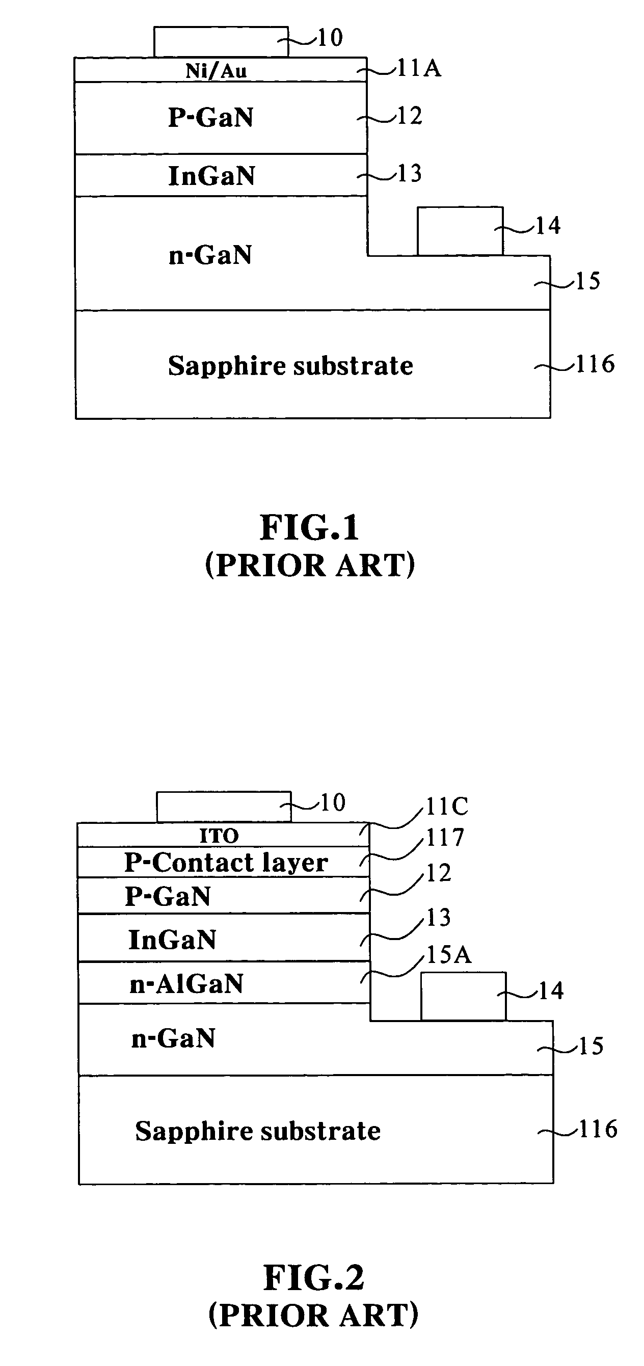
Such poor conductivity cannot effectively distribute the current to the entire p-type compound semiconductor layer.
So, it is unstable and unreliable in high humidity condition.

Method used


Image

  • High brightness gallium nitride-based light emitting diode with transparent conducting oxide spreading layer
  • High brightness gallium nitride-based light emitting diode with transparent conducting oxide spreading layer
  • High brightness gallium nitride-based light emitting diode with transparent conducting oxide spreading layer

Examples


Embodiment Construction

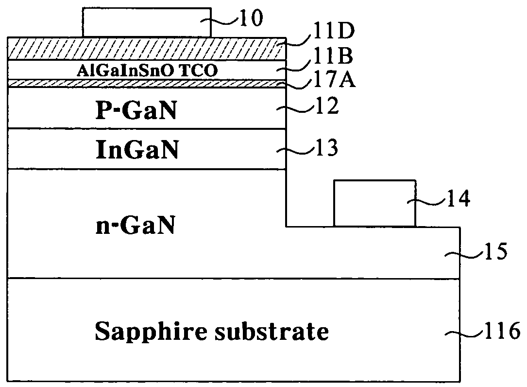
[0030]To prepare the samples under the same thickness condition of an Indium-Tin Oxide (ITO), Ga1.6In6.4Sn2O16, Ga2.8In5.2Sn2O16 and Al0.1Ga2.7In5.2Sn2O16 transparent conducting oxides. The color of the Al2O3—Ga2O3—In2O3—SnO2 system samples ranged from light blue-green (slight Aluminum content) to light green (high Gallium content) to green (low Gallium content). The color of a polycrystalline Indium-Tin Oxide (ITO) sample was also green, but dark than any of the Al2O3—Ga2O3—In2O3—SnO2 system samples.

[0031]FIG. 9 compares the transmittance spectra (UV-V is region) of ITO, Ga1.6In6.4Sn2O16, Ga2.8In5.2Sn2O16 and Al0.1Ga2.7In5.2Sn2O16. Transmittances of the AlxGa3-x-yIn5+ySn2-zO16-2z compositions are slightly superior to Indium-Tin Oxide (ITO) at wavelength (λ)>400 nm, in addition, the AlxGa3-x-yIn5+ySn2-zO16-2z composition have a lower absorption at UV region. The present invention shows, increasing the Gallium concentration or slight Aluminum concentration to AlxGa3-x-yIn5+ySn2-zO16-...


PUM

PropertyMeasurementUnit
thicknessaaaaaaaaaa
thicknessaaaaaaaaaa
thicknessaaaaaaaaaa

Abstract

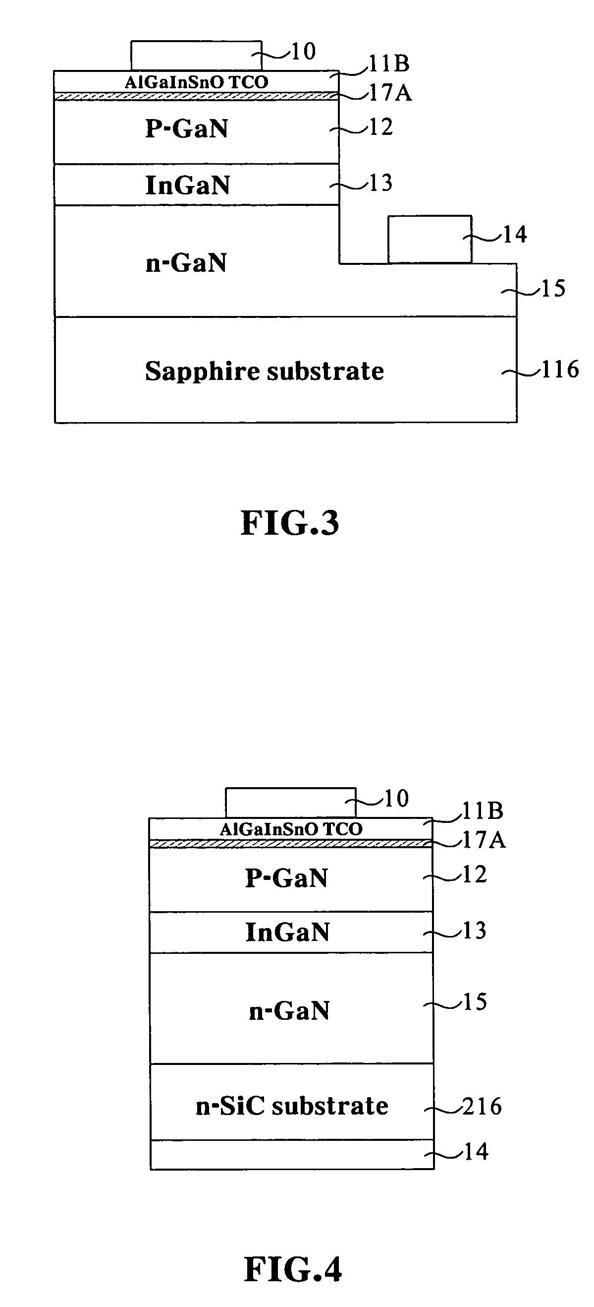
A new transparent conducting oxide (TCO), which can be expressed as AlxGa3-x-yIn5+ySn2-zO16-2z; 0≦x<1, 0<y<3, 0≦z<2, has been used to improve the brightness and current spreading in GaN base LED process. The optical properties of this system are superior to regular Ni / Au transparent conducting layer in blue-green region, and the new Al2O3—Ga2O3—In2O3—SnO2 system is able to increase the brightness at 1.5˜2.5 time to compare to regular process. Furthermore, the new transparent conducting oxide thin film has the highest conductivity, which is better than the Ni / Au transparent conducting thin film.

Description

BACKGROUND OF THE INVENTION[0001]1. Field of the Invention[0002]The present invention relates to the field of transparent conducting oxide (TCO) and solid-state Gallium Nitride-based light-emitting devices.[0003]2. Description of the Related Art[0004]In recent years, the p-type Gallium Nitride-based III-V group compound semiconductor layer usually has a carrier concentration of less than 1×1018 cm−3, and the lowest resistivity is no lower than 1 ohm-cm. Such poor conductivity cannot effectively distribute the current to the entire p-type compound semiconductor layer. Therefore, the p-electrode is usually formed to cover substantially entire surface of the p-type Gallium Nitride-based III-V group compound semiconductor layer in order to ensure the uniform spreading of current to the entire p-type compound semiconductor layer, thereby obtaining uniform light emission from the device. However, the p-electrode considered being a light transmitting and ohmic electrode.[0005]Due to the en...

Claims


Application Information

Patent Timeline
Patent Type & Authority Patents(United States)
IPC IPC(8): H01L33/00H01L31/109H01L33/14H01L33/32H01L33/42
CPCH01L33/14H01L33/42H01L33/32D06M11/42D06P1/34D03D15/247D03D15/258
Inventor HUANG, WEN-CHIEH
Owner ARIMA OPTOELECTRONICS
Learn More