
Athermal AWG and AWG with low power consumption using groove of changeable width

Inactive Publication Date: 2006-06-13
NEOPHOTONICS CORP
View PDF17 Cites 21 Cited by
  • Summary
  • Abstract
  • Description
  • Claims
  • Application Information

AI Technical Summary

Benefits of technology

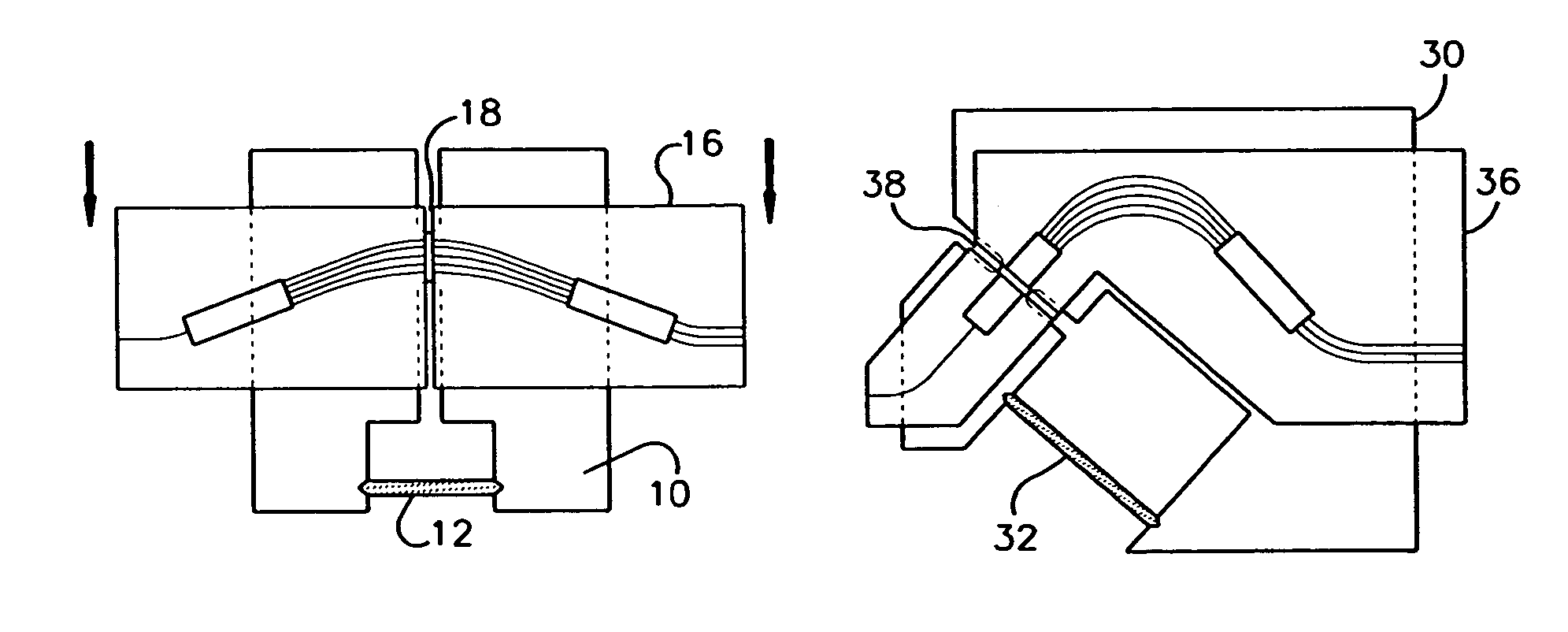
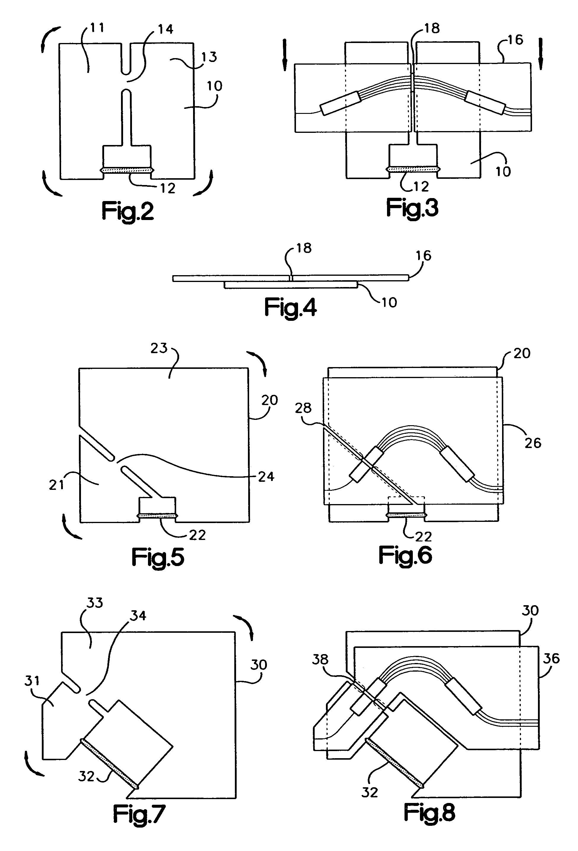
[0011]The present invention provides athermal optical integrated circuits and methods for athermalizing optical integrated circuits mitigating and / or overcoming the shortcomings associated with conventional optical integrated circuit(s) and other devices. The invention further comprises methods for fabricating OICs and for mitigating temperature sensitivity utilizing a groove and an actuator. Markedly lower power consumption also results from employing temperature responsive mechanical actuators in another aspect of the present invention.
[0012]According to an aspect of the present invention, an optical integrated circuit is provided that contains a base containing a first region and a second region separated by a hinge, and an AWG chip over the base, where a groove traverses one or more of one of the lenses and the waveguide grating, and an actuator connecting the first region and the second region of the base. The base and actuator have different thermal expansion coefficients. The actuator expands and / or contracts with temperature changes causing the first region and at least a portion of the AWG chip thereover to move with respect to the portion of the AWG chip over the second region. Thus, wavelength shift associated with waveguide temperature dependent refractive index can be mitigated.
[0013]According to another aspect of the present invention, optical integrated circuit is provided that contains an AWG chip with a groove traversing one or more of the lenses and the waveguide grating. The AWG chip contains a first region and a second region connected by a hinge and separated by the groove. An actuator connects the first region and the second region of the AWG chip. The AWG chip substrate and actuator have different thermal expansion coefficients. The actuator expands and / or contracts with temperature changes causing the first region of the AWG chip to move with respect to the second region. Thus, wavelength shift associated with waveguide temperature dependent refractive index can be mitigated.

Problems solved by technology

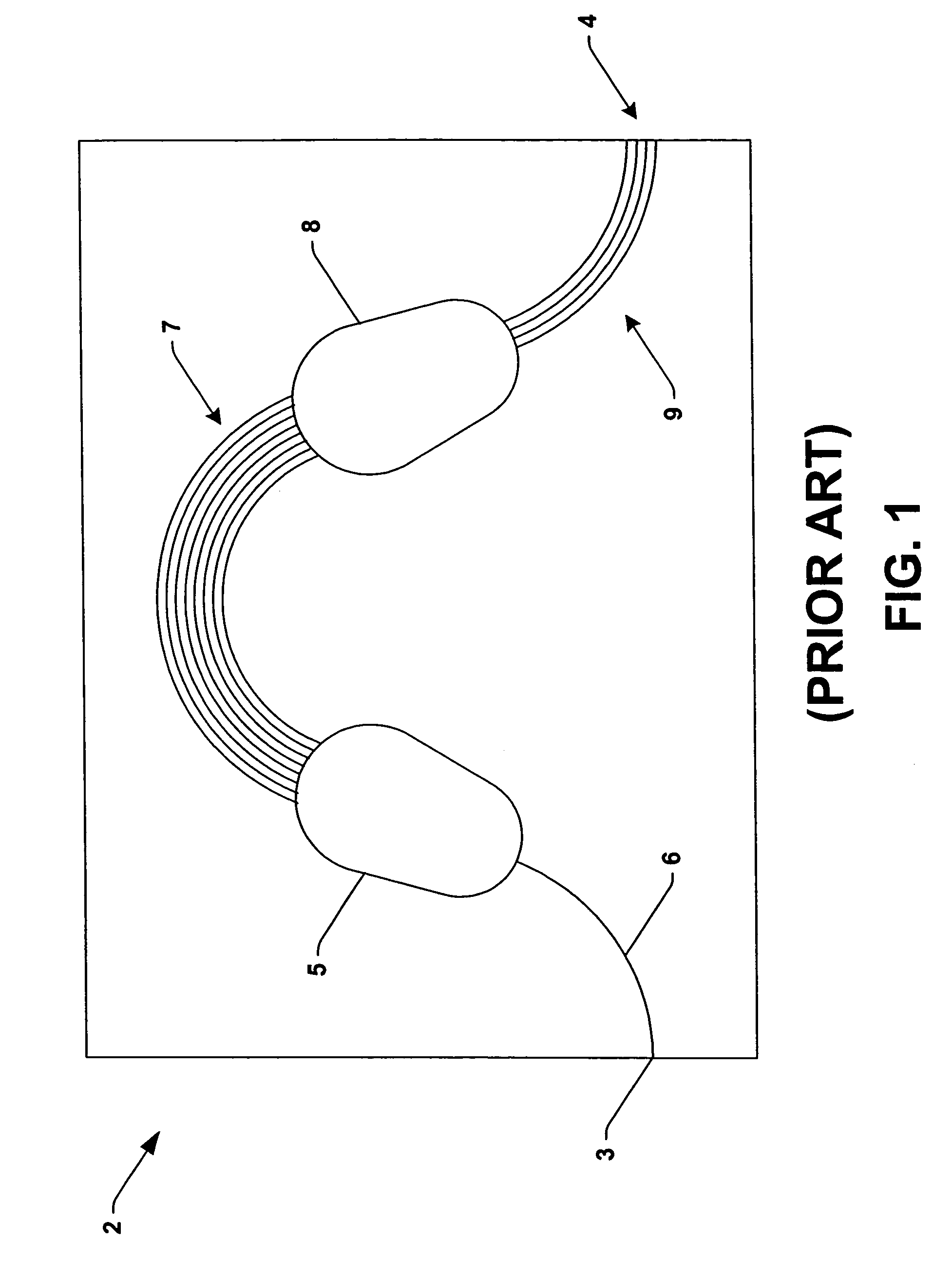
One of the problems with optical integrated circuits, such as the conventional AWG 2 of FIG. 1 is temperature sensitivity.
This wavelength shift can result in a loss of signal and / or cross talk in communication system(s) employing the AWG 2.
Even though an AWG is a passive filter, currently it requires significant electronics and a few watts of power to operate effectively.

Method used


Image

  • Athermal AWG and AWG with low power consumption using groove of changeable width
  • Athermal AWG and AWG with low power consumption using groove of changeable width
  • Athermal AWG and AWG with low power consumption using groove of changeable width

Examples


Embodiment Construction

[0035]The various aspects of the present invention will now be described with reference to the drawings, wherein like reference numerals are used to refer to like elements throughout. The invention provides for mitigation of temperature sensitivity of optical integrated circuits by employing mechanical beam steering.

[0036]The present invention provides athermal OICs and OICs with low power consumption by employing beam deflection, using an OIC or AWG having two or more distinct regions or pieces that can move relative to one another. This relative movement causes shifts in the center wavelength (CW), or wavelength of peak transmission for a given channel, of the OIC that are proportional to the motion of the two pieces. The OIC is designed such that the degree of CW change caused by the motion of the two pieces is equal in magnitude and opposite in sign to the CW change inherent in the OIC (as caused by expansion / contraction of the OIC and dependencies of waveguide refractive index ...


PUM


Abstract

Optical integrated circuits are disclosed having a gap traversing the lens or the waveguide grating and an actuator that controllably positions the optical integrated circuit on each side of the gap. As a result, the thermal sensitivity of the optical integrated circuits, for example, arrayed waveguide gratings, is mitigated. Also disclosed are methods for fabricating optical integrated circuits employing the gap and actuator.

Description

[0001]This patent application is a continuation of application Ser. No. 10 / 100,958 filed on Mar. 18, 2002, now U.S. Pat. No. 6,738,545.FIELD OF THE INVENTION[0002]The present invention relates to the art of optical integrated circuits and more particularly to apparatus and methods for providing arrayed waveguides having a center wavelength that is independent of temperature.BACKGROUND OF THE INVENTION[0003]Optical integrated circuits (OICs) come in many forms such as 1×N optical splitters, optical switches, wavelength division multiplexers (WDMs), demultiplexers, optical add / drop multiplexers (OADMs), and the like. Such OICs are employed in constructing optical networks in which light signals are transmitted between optical devices for carrying data and other information. For instance, traditional signal exchanges within telecommunications networks and data communications networks using transmission of electrical signals via electrically conductive lines are being replaced with opti...

Claims


Application Information

Patent Timeline
IPC IPC(8): G02B6/34G02B6/35
CPCG02B6/12011G02B6/1203G02B6/12014
Inventor PURCHASE, KENNETHCOLE, ROBERTTICKNOR, ANTHONY J.MCGREER, KENNETHASCANIO, PETER D.
Owner NEOPHOTONICS CORP
Learn More