High voltage, low-offset operational amplifier with rail-to-rail common mode input range in a digital CMOS process

a technology of digital cmos and operational amplifiers, applied in the field of analog circuits, can solve the problems of low-offset operational amplifiers, and achieve the effects of reducing the number of discrete devices, reducing the cost of manufacture, and reducing the size of the devi

Active Publication Date: 2006-06-20
SEMICON COMPONENTS IND LLC
View PDF5 Cites 23 Cited by
  • Summary
  • Abstract
  • Description
  • Claims
  • Application Information

AI Technical Summary

Benefits of technology

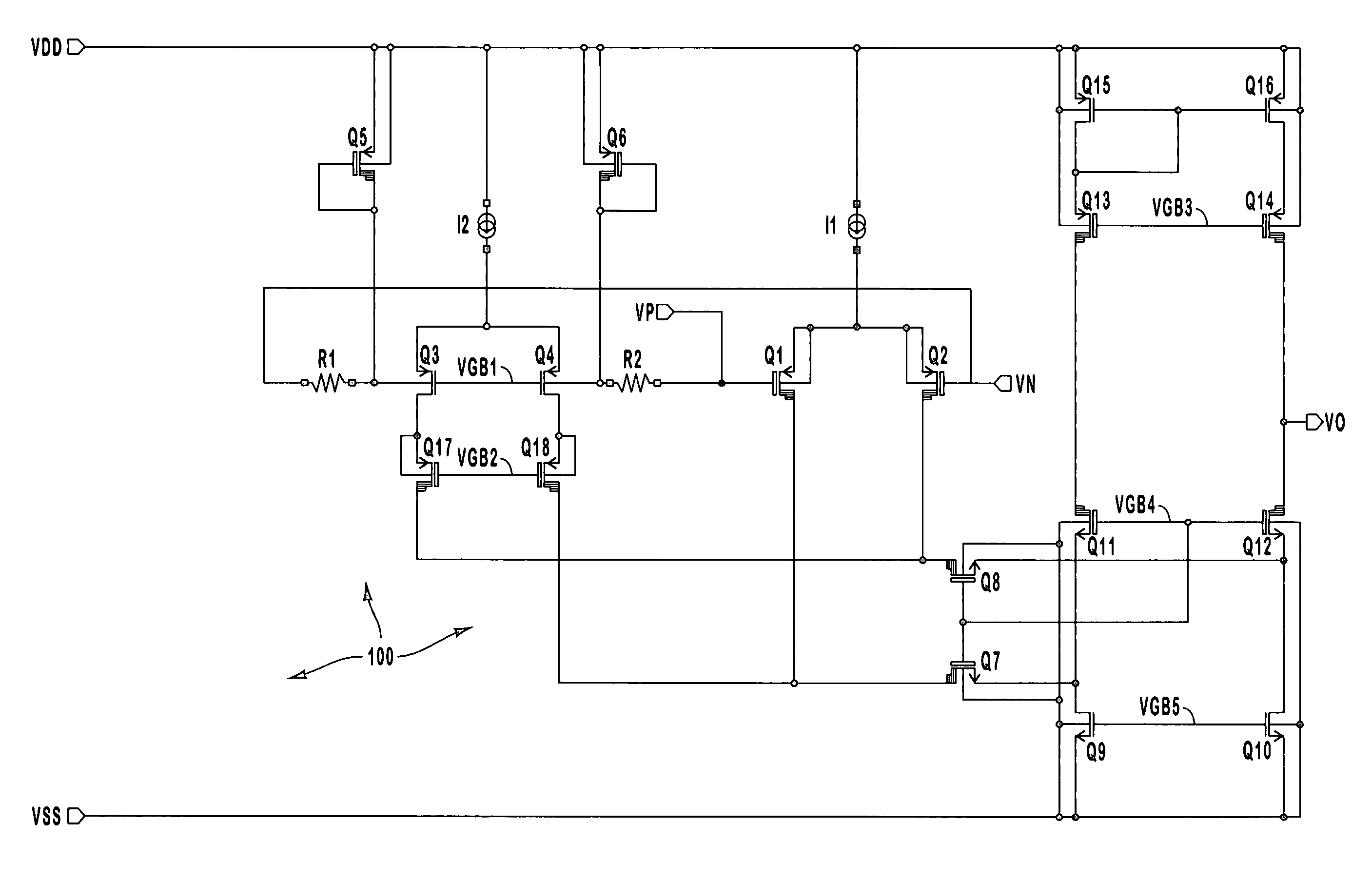
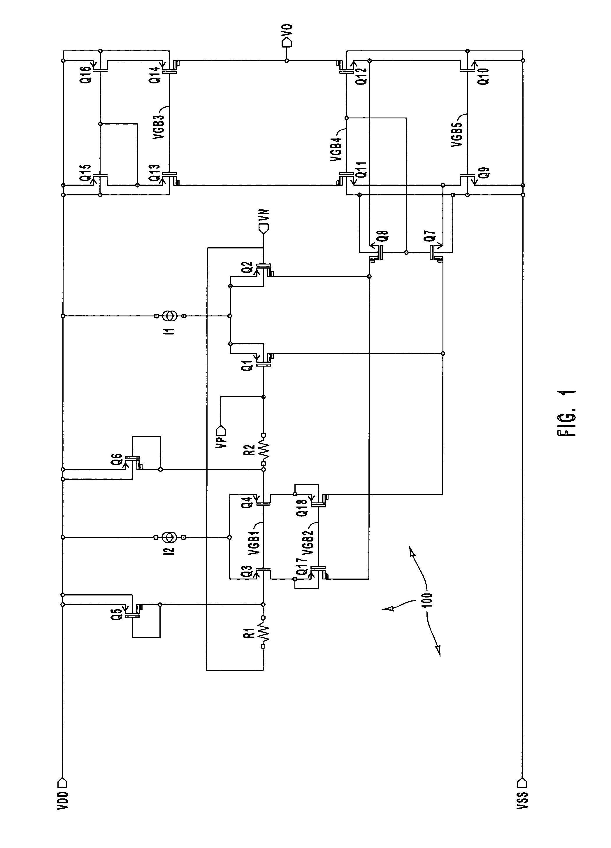
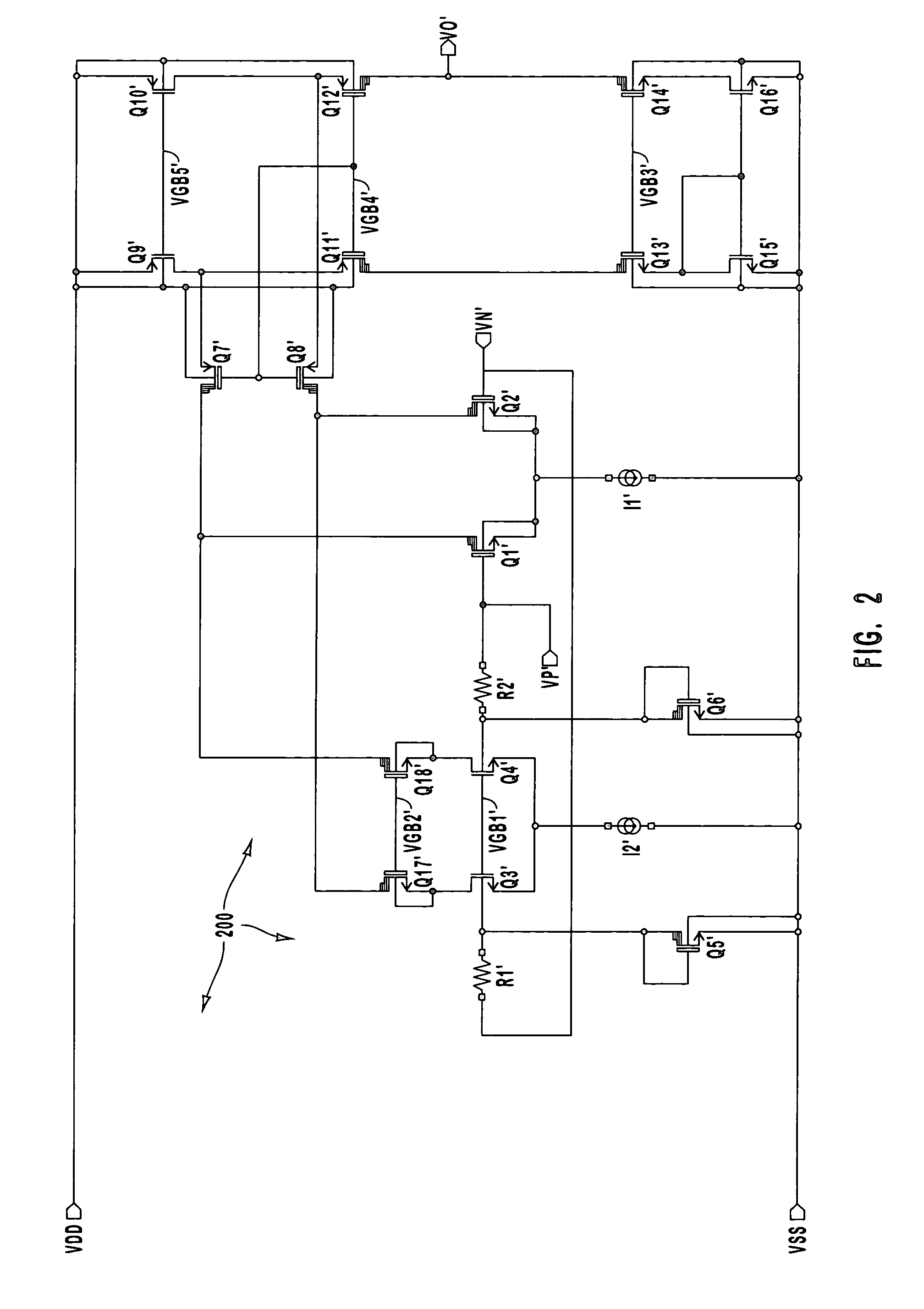
[0013]The gate terminal of a first field effect transistor in the first differential pair is coupled to the positive input terminal. A gate terminal of the second field effect transistor in the first differential pair is coupled to the negative input terminal. In accordance with a first embodiment of the invention, the bulk terminal of the first field effect transistor in the second differential pair is coupled to the negative input terminal. Furthermore, the bulk terminal of the second field effect transistor in the second differential pair is coupled to the positive input terminal. In accordance with a second embodiment of the invention, the second differential pair includes gate driven depletion type transistors. The gate terminal of the first depletion type field effect transistor in the second differential pair is coupled to the negative input terminal. Furthermore, the gate terminal of the second depletion type field effect transistor in the second differential pair is coupled to the positive input terminal.
[0014]The first differential pair is used for common mode input range for most of the rail-to-rail voltage, while the second differential pair is used for common mode input range for the remainder of the rail-to-rail voltage. Accordingly, full rail-to-rail common mode input range is accomplished. Furthermore, by using the bulk terminals of the field effect transistors in the second differential pair as the input terminal, rather than using the gate terminals as the input terminal, the operational amplifier may be constructed using a single well process, thereby being compatible with standard digital CMOS processes. The single well process is also possible in the second embodiment when driving the gate terminals of the depletion type transistors, although an additional depletion mode implant would typically be used.
[0015]The use of the single well process allows the high voltage amplifier to be constructed on the same chip as digital circuitry thereby reducing the number of discrete devices. This reduces the cost of manufacture for the digital circuitry, reduces its size, and increases its reliability. Additionally, high voltage field effect transistors may be used so that the second differential pair may be composed of standard field effect transistors that typically have better matching characteristics than high voltage field effect transistors. The use of the high voltage field effect transistors in conjunction with the standard low voltage field effect transistors results in lower operational amplifier offset. Accordingly, the principles of the present invention provide for a high voltage, low-offset rail-to-rail common mode input range operational amplifier that is compatible with standard digital CMOS processes.
[0016]The operational amplifier may also include an output stage as well as a coupling stage for coupling the input stage and the output stage. In the output stage, two standard low voltage field effect transistors serve as a dual current source (or sink). A high voltage field effect transistor is coupled between the output terminal and each of the low voltage current source (or sink) field effect transistors. This configuration may be present between the output terminal and the high supply voltage as well as between the output terminal and the low supply voltage. This configuration in the output stage further reduces the offset of the operational amplifier.

Problems solved by technology

The use of the high voltage field effect transistors in conjunction with the standard low voltage field effect transistors results in lower operational amplifier offset.

Method used


Image

  • High voltage, low-offset operational amplifier with rail-to-rail common mode input range in a digital CMOS process
  • High voltage, low-offset operational amplifier with rail-to-rail common mode input range in a digital CMOS process
  • High voltage, low-offset operational amplifier with rail-to-rail common mode input range in a digital CMOS process

Examples


Embodiment Construction

[0024]The principles of the present invention relate a high-voltage operational amplifier that has low-offset and wide common-mode input range and that may be integrated in a single-well CMOS process, thereby being compatible with standard digital CMOS processes.

[0025]One of the limitations of high voltage devices in a standard digital CMOS process is that the maximum gate-bulk voltage is much less than the maximum drain-bulk voltage. This means that if high voltage devices are used as the differential input devices, the input range will be constrained by the maximum gate-bulk voltage.

[0026]High voltage amplifiers often use feedback to assure that each device is within its safe operating area. Referencing FIG. 5, it is apparent that that as the voltage changes on the gates of devices Q501, Q502, Q503 and Q504, voltage nodes VSP and VSN change with the gate voltage, keeping the gate-source voltage and gate-bulk voltage within their breakdown voltages.

[0027]However, in the case of a s...


PUM


Abstract

An operational amplifier with two differential pairs coupled to different current sources. The gate terminals of the transistors in the first differential pair are used as input terminals providing common mode input for most of the rail-to-rail voltage. The bulk terminals of the transistors in the second differential pair are used as input terminals providing common mode input for the remainder of the rail-to-rail voltage to thereby accomplish full rail-to-rail common mode. By using the bulk terminals of the field effect transistors in the second differential pair, rather than the gate terminals, as the input terminal, the operational amplifier may be constructing in a single well, thereby being compatible with standard digital CMOS processes. Alternatively, the bulk-driven transistors may be replaced with gate-driven depletion type transistors. The high voltage transistors in the output stage further reduce the offset voltage of the operational amplifier.

Description

BACKGROUND OF THE INVENTION[0001]1. The Field of the Invention[0002]The present invention relates generally to analog circuits. More specifically, the present invention relates to high-voltage, low-offset operational amplifiers with rail-to-rail common mode input range that may be implemented using a digital CMOS process.[0003]2. Background and Relevant Art[0004]Electronic circuitry provides complex functionality that is proving ever more useful. Electronic circuitry pervades our modern lives in areas such as communication, entertainment, travel, productivity, and the like. Complex circuit functionality is enabled by cooperative interaction between a variety of electronic components. Such electronic components may include analog components such as, for example, operational amplifiers, as well as digital circuitry. It is ever more desirable to integrate as many electronic components as possible on a single chip. This reduces the number of discrete components required to accomplish ce...

Claims


Application Information

Patent Timeline
Patent Type & Authority Patents(United States)
IPC IPC(8): H03F3/45
CPCH03F3/3022H03F3/45188H03F3/45744H03F2203/45681H03F2203/45214H03F2203/45342H03F2203/45366H03F2203/45212
Inventor BECK, RILEY D.SHREEVE, AARON M.
Owner SEMICON COMPONENTS IND LLC
Why Eureka
Try Eureka