Thin-film common mode filter and thin-film common mode filter array

a filter array and common mode technology, applied in the direction of impedence networks, inductances with magnetic cores, inductances, etc., can solve the problems preventing insulation failures, and achieve the effect of lowering the reliability of conduction

Active Publication Date: 2006-06-20
TDK CORPARATION
View PDF7 Cites 23 Cited by
  • Summary
  • Abstract
  • Description
  • Claims
  • Application Information

AI Technical Summary

Benefits of technology

[0008]It is therefore an object of the present invention to provide a thin-film common mode filter and a thin-film common mode filter array that can prevent the lowering of the reliability in conduction and the insulation failure in the connection portion between the upper coil conductor and the upper lead conductor.
[0010]By setting the pedestal part below the contact hole between the upper coil conductor and the upper lead conductor, and then lifting up the insulating bottom portion underneath the contact hole as much as possible, a disadvantage such as a lowering reliability in conduction and an insulation failure can be prevented.
[0012]It is also preferable that widths (W1) of the upper lead conductor and the lower lead conductor are less than twice the widths (W2) of the upper coil conductor and the lower coil conductor (W1<2W2). As described above, the higher aspect ratios (height / width) of the coil pattern and of the lead pattern in the thin-film common mode filter cause smaller capacities between the coil conductors and between the coil conductor and the lead conductor. As the results, the high-frequency transmission properties are improved. However, the high aspect ratio design makes it difficult to narrow spacings between the lead conductors and the coil conductors. To solve the difficulty, narrowing widths of the lead conductors is effective. In fact, setting the widths of the lead conductors (W1) not less than twice the widths of the coil conductors (W2) decrease the resonance frequency to a large degree. Therefore, by setting W1<2W2, the thin-film common mode filter showing less decrease in the resonance frequency can be provided.

Problems solved by technology

By setting the pedestal part below the contact hole between the upper coil conductor and the upper lead conductor, and then lifting up the insulating bottom portion underneath the contact hole as much as possible, a disadvantage such as a lowering reliability in conduction and an insulation failure can be prevented.

Method used


Image

  • Thin-film common mode filter and thin-film common mode filter array
  • Thin-film common mode filter and thin-film common mode filter array
  • Thin-film common mode filter and thin-film common mode filter array

Examples


Embodiment Construction

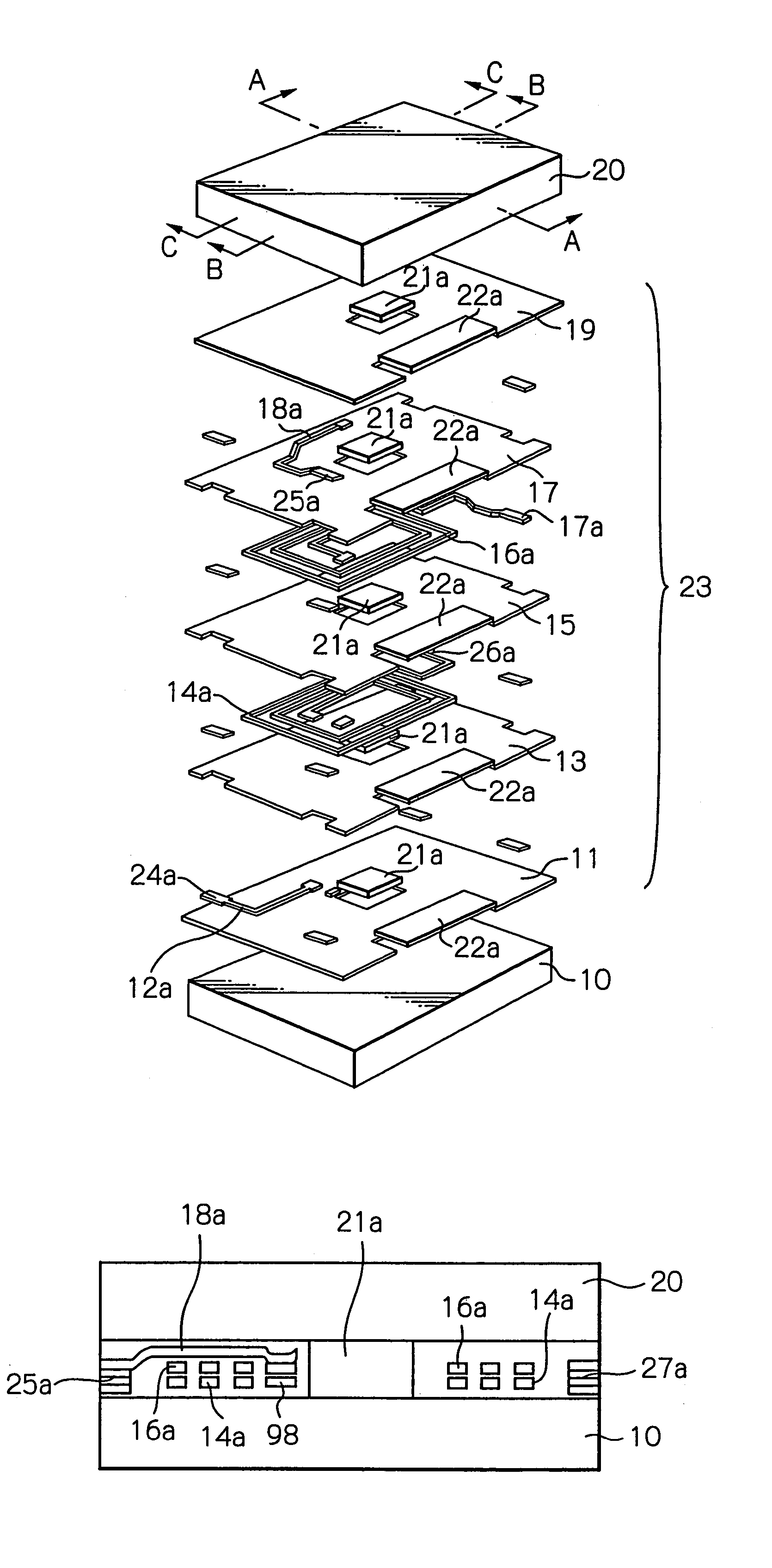
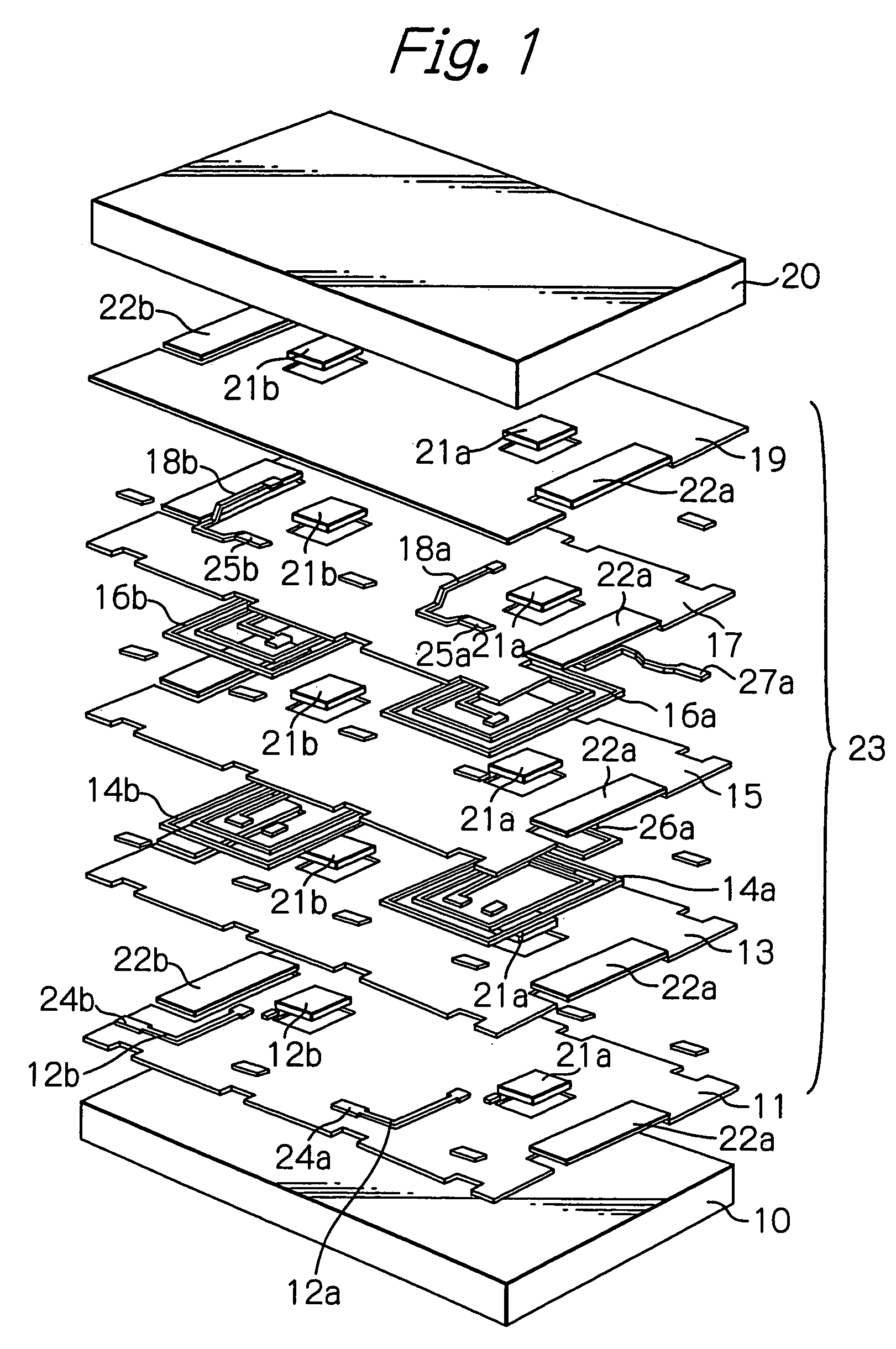
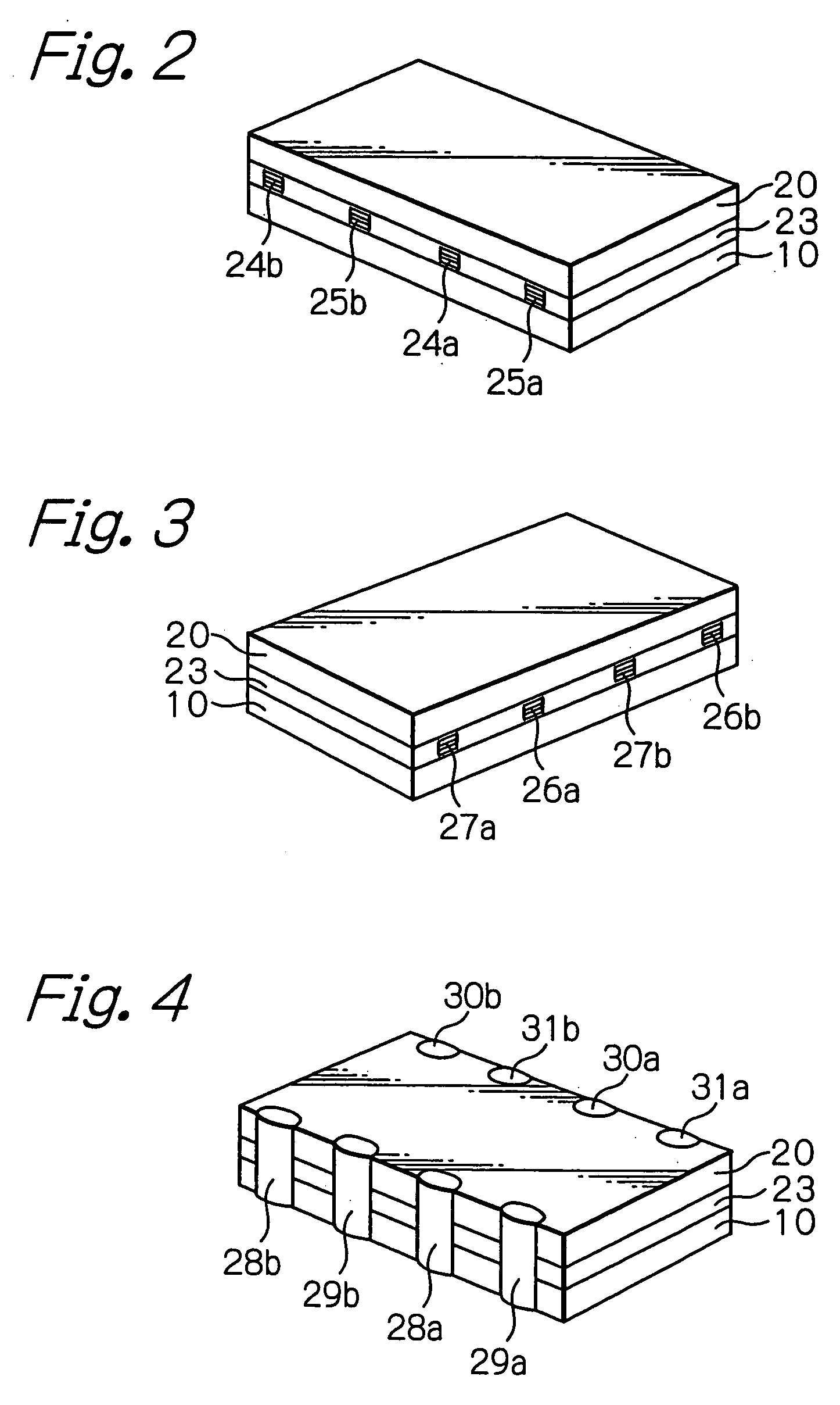
[0029]FIG. 1 shows an exploded perspective view schematically illustrating a structure of a thin-film common mode filter array according to an embodiment of the present invention. FIG. 2 shows a perspective view schematically illustrating an appearance of a thin-film common mode filter array when cut out of a wafer. FIG. 3 shows another perspective view from the different direction from that in FIG. 2, schematically illustrating an appearance of a thin-film common mode filter array when cut out of a wafer. FIG. 4 shows a perspective view schematically illustrating an appearance of a finished-up thin-film common mode filter array.

[0030]The thin-film common mode filter array is formed as a chip by aligning two thin-film common mode filters.

[0031]In FIG. 1, reference numeral 10 indicates an insulating magnetic substrate, 11 indicates a first insulating layer usually formed of a polyimide or a BCB (benzocyclobutene) that have great heat-resistance, stacked on the insulating magnetic sub...


PUM

PropertyMeasurementUnit
resonance frequencyaaaaaaaaaa
widthsaaaaaaaaaa
High-frequency propertiesaaaaaaaaaa

Abstract

A thin-film common mode filter is provided, comprising: a pair of magnetic plates; an upper coil conductor and a lower coil conductor formed between the pair of magnetic plates, spirally wound in the magnetic plate surface direction, and overlapped each other; an upper lead conductor and a lower lead conductor, one ends of the upper lead conductor and the lower lead conductor connected electrically to one ends in center portions of the upper coil conductor and the lower coil conductor, respectively, and extended to external portions across the upper coil conductor and the lower coil conductor; and a pedestal part formed below a connection portion between the upper coil conductor and the upper lead conductor, for lifting the connection portion to an upper position.

Description

PRIORITY CLAIM[0001]This application claims priority from Japanese patent application No. 2003-398965, filed on Nov. 28, 2003, which is incorporated herein by reference.BACKGROUND OF THE INVENTION[0002]1. Field of the Invention[0003]The present invention relates to a thin-film common mode filter and a thin-film common mode filter array.[0004]2. Description of the Related Art[0005]Common mode filter is a device for suppressing common mode currents that cause electromagnetic interference in parallel transmission lines. The common mode filter has magnetically coupled inductors to remove in-phase noise component.[0006]Thin-film common mode filter miniaturized and highly integrated by forming bilayered thin-film coils between ferrite substrates and by constructing in chip form, and thin film common mode filter array on which a plurality of the filters are mounted, are described in for example, Japanese Patent Publications Nos. 04-364709A, 08-203737A, 08-335517A and 11-054326A.[0007]High-...

Claims


Application Information

Patent Timeline
Patent Type & Authority Patents(United States)
IPC IPC(8): H03H7/01H01F17/00H01F5/00H01F17/04H01F27/29H04B15/02
CPCH04B15/02
Inventor SHOJI, SHIGERU
Owner TDK CORPARATION
Why Eureka
Try Eureka