
Automated repetitive array microstructure defect inspection

a technology of repetitive arrays and defects, applied in the field of automatic repetitive array microstructure defect inspection, can solve the problems of increasing the sensitivity of array mode defects, affecting the accuracy of real 100% continuous defects, and reducing the actual area of true 100% continuous accurately repetitive areas, so as to reduce the impact of problems.

Inactive Publication Date: 2006-06-20
APPLIED MATERIALS INC
View PDF10 Cites 71 Cited by
  • Summary
  • Abstract
  • Description
  • Claims
  • Application Information

AI Technical Summary

Benefits of technology

[0019]In view of the above problems, an object of the present invention is to provide a method and system apparatus for rapidly and thoroughly inspecting microfabricated structures with repetitive arrays while eliminating or minimizing the impact of the problems and limitations described.

Problems solved by technology

This results in increased sensitivity to defects in array mode inspection (versus random mode inspection).
However, this approach to inspecting array or repetitive areas and the approach used on commercial defect inspection systems available today have some important disadvantages, specifically:the edges of the repetitive array area must be defined manually before inspection.
This can be and often is an extremely time consuming and tedious process especially on advanced memory ICs where the actual area of truly 100% continuous accurately repetitive areas is rather limited.
Each truly repetitive array segment must be identified manually before inspection.adjoining non-repetitive segments must be inspected with a separate inspection algorithm for random areas requiring a time consuming second pass of the inspection tool effectively cutting actual tool throughput by 50% or more.array edges are often not inspected as the accuracy of definition of the array boundaries is limited by inspection system overall position accuracy (stage errors, encoder errors, alignment errors and other error sources combined) and must include a buffer or exclusion zone at the edge of the array to ensure that false defect counts or false alarms are not generated when inadvertently inspecting non-repetitive regions surrounding the repetitive regions when for example accuracy limits are reached.

Method used


Image

  • Automated repetitive array microstructure defect inspection
  • Automated repetitive array microstructure defect inspection
  • Automated repetitive array microstructure defect inspection

Examples


Embodiment Construction

[0041]In the following detailed description of the preferred embodiments and other embodiments of the invention, reference is made to the accompanying drawings. It is to be understood that those of skill in the art will readily see other embodiments and changes may be made without departing from the scope of the invention.

[0042]The following terms are defined below for clarification and are used to describe the drawings and embodiments of the invention:

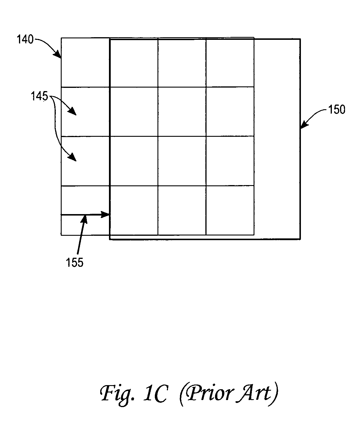
[0043]Cell: A single cell repeated in a microfabricated structure such as for example, a DRAM or SRAM cell (or multiples there of) in a semiconductor wafer. This may include macro-cells comprised of multiple cells reflected and combined in groups of two, four or more cells together.

[0044]Cell size: The size of the repeating cell in the X direction or Y direction usually measured in microns or pixels and sometimes also reported as a spatial frequency, for example, as a number of cells per unit length.

[0045]Array (of cells): An area of ...


PUM


Abstract

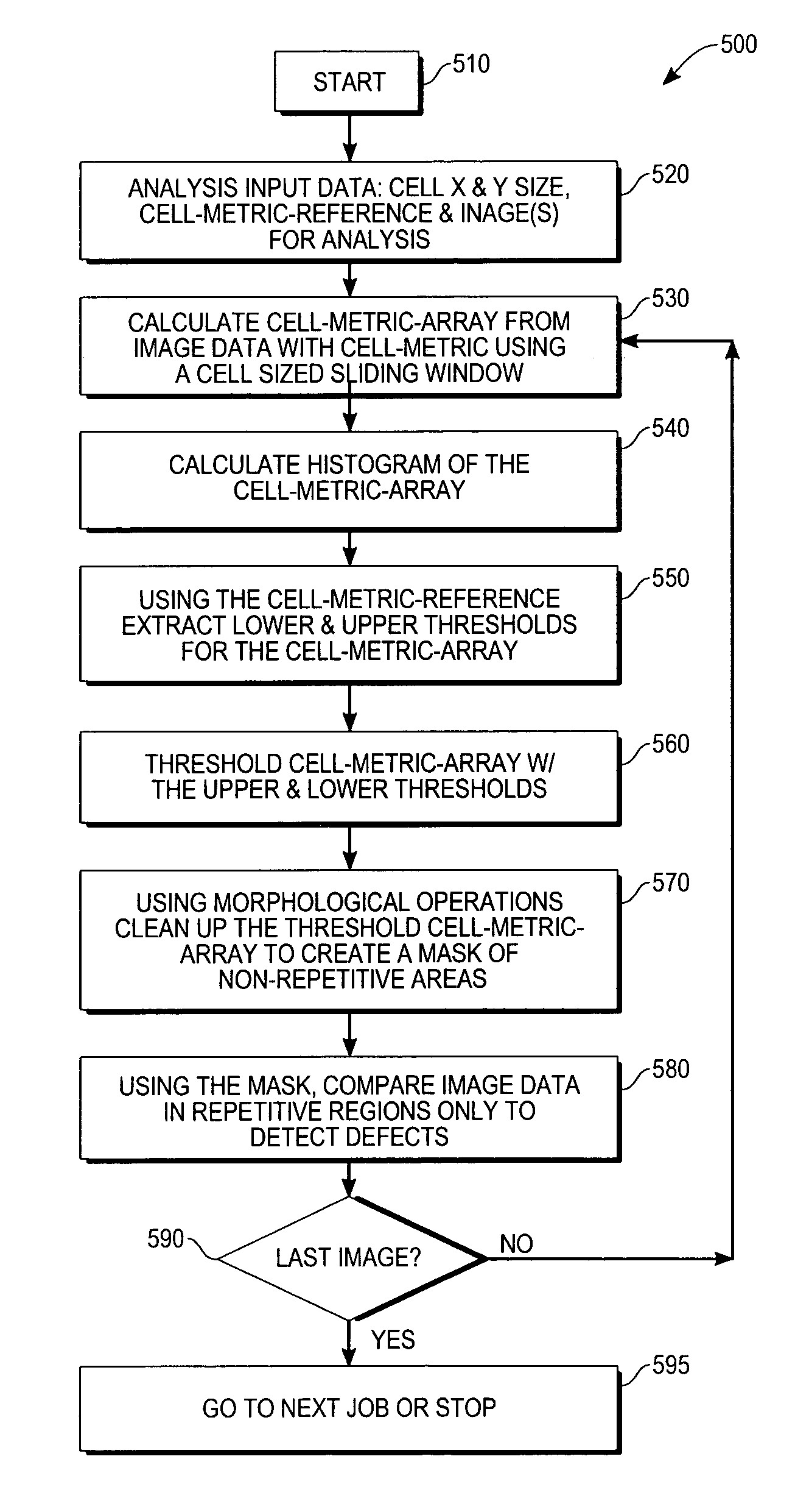
A method and system for defect inspection of microfabricated structures such as semiconductor wafers, masks or reticles for micro-fabrication, flat panel displays, micro-electro-mechanical (MEMs) having repetitive array regions such as memories or pixels. In one embodiment a method of inspection of microfabricated structures includes the steps of acquiring contrast data or images from the microfabricated structures, analyzing automatically the contrast data or images to find repetitive regions of the contrast data and comparing the repetitive regions of the contrast data with reference data to detect defects in the microfabricated structures. In the analyzing step, a cell-metric such as the range, or mean or other statistical or mathematical measure of the contrast data is used to find the repetitive regions. Image or contrast data acquisition can be performed with an optical, e-beam or other microscope suited for microfabricated structures.

Description

BACKGROUND OF INVENTION[0001]1. Field of the Invention[0002]This invention relates to methods and systems for use in defect inspection of microfabricated structures such as integrated circuit die on semiconductor wafers, masks or reticles for microfabrication, flat panel displays, micro-electromechanical (MEMs) devices and the like during and after manufacture. In particular, the invention provides methods and systems for more effectively and efficiently inspecting microfabricated structures that are repetitive in nature such as memory cells including SRAM, DRAM, FRAM, Flash memory, repetitive programmable logic ICs such as PLAs, PLDs, MEMs displays repetitive pixel structures and flat panel displays with repetitive pixel structures and the like.[0003]2. Prior Art[0004]Over the past decade, defect inspection to detect microscopic manufacturing defects has become a standard part of microfabrication manufacturing flows, especially for semiconductor wafers.[0005]Various types of inspec...

Claims


Application Information

Patent Timeline
IPC IPC(8): G06K9/00G06T7/00
CPCG06T7/0004G06T2207/30148
Inventor MAAYAH, KAIS JAMEELGALLARDA, JR., HARRY STANTONSRINIVASAN, LAKSHMANBARNARD, RICHARDLIU, JUN
Owner APPLIED MATERIALS INC
Learn More