Electrical die contact structure and fabrication method

a technology of contact structure and die, applied in the direction of semiconductor devices, semiconductor/solid-state device details, electrical apparatus, etc., can solve the problems of prone to bad bond formation of bonding and tab bonding, high temperature and mechanical pressure on the die, and the above-described technologies have certain limitations

Inactive Publication Date: 2006-06-27
NAT SEMICON CORP
View PDF5 Cites 41 Cited by
  • Summary
  • Abstract
  • Description
  • Claims
  • Application Information

AI Technical Summary

Problems solved by technology

Each of the above-described technologies has certain limitations.
Both wire bonding and TAB bonding are prone to bad bond formation and subject the die to relatively high temperatures and mechanical pressures.
Additionally, wire bond and TAB technologies are problematic from a package size viewpoint, producing integrated circuit devices having a die-to-package area ratio ranging from about 10% to 60%.
However, flip-chip interconnection suffers from a number of limitations.
For example, variations in solder bump uniformity and thermal expansion mismatching present problems.
These difficulties limit the use of available substrates to silicon materials or materials which have thermal expansion characteristics simil

Method used


Image

  • Electrical die contact structure and fabrication method
  • Electrical die contact structure and fabrication method
  • Electrical die contact structure and fabrication method

Examples


Embodiment Construction

[0032]The present invention has been particularly shown and described with respect to certain embodiments and specific features thereof. The embodiments set forth hereinbelow are to be taken as illustrative rather than limiting. It should be readily apparent to those of ordinary skill in the art that various changes and modifications in form and detail may be made without departing from the spirit and scope of the invention.

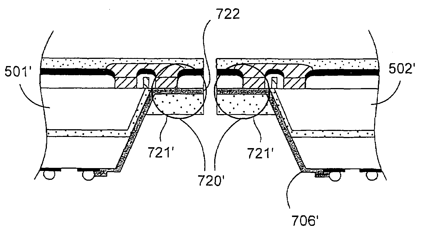
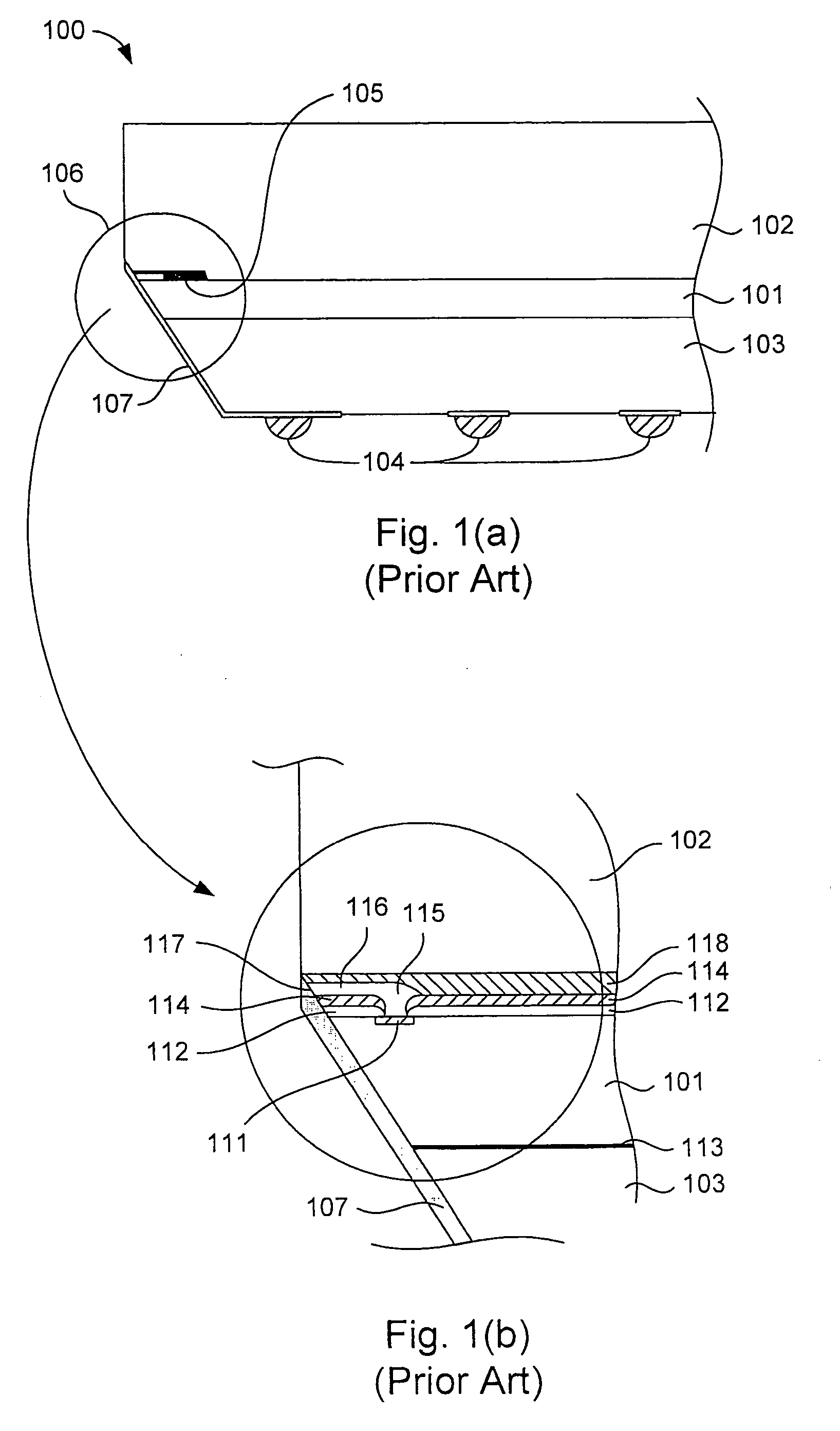
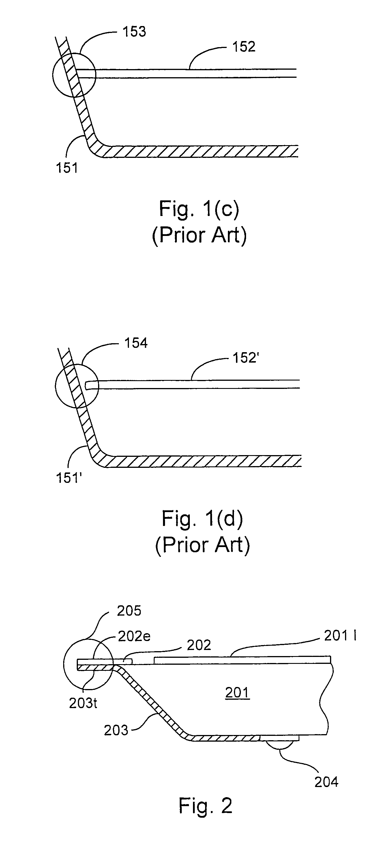
[0033]One aspect of the invention includes the fabrication and implementation of a semiconductor die having a plurality of robust edge mounted electrical connectors (also referred to herein as lap joint electrical connectors or lap joints). FIG. 2 depicts a generalized implementation of the principles of the invention. A semiconductor substrate 201 has integrated circuit structures 201I formed thereon. The integrated circuit structures 201I are electrically connected to a contact pad 202. The contact pad 202 includes a contact pad extension 202e that extends beyo...


PUM


Abstract

A semiconductor device of the invention includes an integrated circuit formed on a semiconductor substrate having first and second surfaces and edges. The first surface includes electrical contact pads electrically connected with the integrated circuit. The first surface of the semiconductor substrate includes a top protective layer that has a surface portion extending beyond the edges of the semiconductor substrate. The surface portion of the top protective layer includes electrical contact pads that are electrically connected with electrical contact pad extensions and with the integrated circuit. The second surface of the semiconductor substrate includes a multiplicity of backside electrical connectors that are in overlapping electrical contact with corresponding electrical contact pad extensions forming lap joint electrical connections between the backside electrical connectors and the corresponding electrical contact pad extensions. Methods for constructing such devices and connections are also disclosed.

Description

RELATED APPLICATIONS[0001]This application is a continuation-in-part of U.S. patent application Ser. No. 10 / 145,295, entitled “Electrical Die Contact Structure and Fabrication Method”, by Prabhu et al., filed on May 13, 2002 which is hereby incorporated by reference in its entirety for all purposes. This application is also a divisional of U.S. patent application Ser. No. 10 / 310,724, entitled “Electrical Die Contact Structure and Fabrication Method”, by Ashok Prabhu, filed on Dec. 4, 2002 now U.S. Pat. No. 6,781,244 which is hereby incorporated by reference in its entirety for all purposes.TECHNICAL FIELD[0002]The invention described herein relates generally to semiconductor chip manufacturing processes. In particular, the invention relates to improved electrical contact structures and the methods for their manufacture.BACKGROUND[0003]One step in the manufacture of integrated circuit devices is known as “packaging” and involves mechanical and environmental protection of a semiconduc...

Claims


Application Information

Patent Timeline
IPC IPC(8): H01L21/44H01L23/48H01L23/482H01L23/52H01L29/04
CPCH01L23/482H01L27/14618H01L23/4827H01L2924/0002H01L2924/00
Inventor PRABHU, ASHOK
Owner NAT SEMICON CORP
Why Eureka
Try Eureka