High-density architecture for a microelectronic complex on a planar body
- Summary
- Abstract
- Description
- Claims
- Application Information
AI Technical Summary
Benefits of technology
Problems solved by technology
Method used
Image

Examples
Embodiment Construction
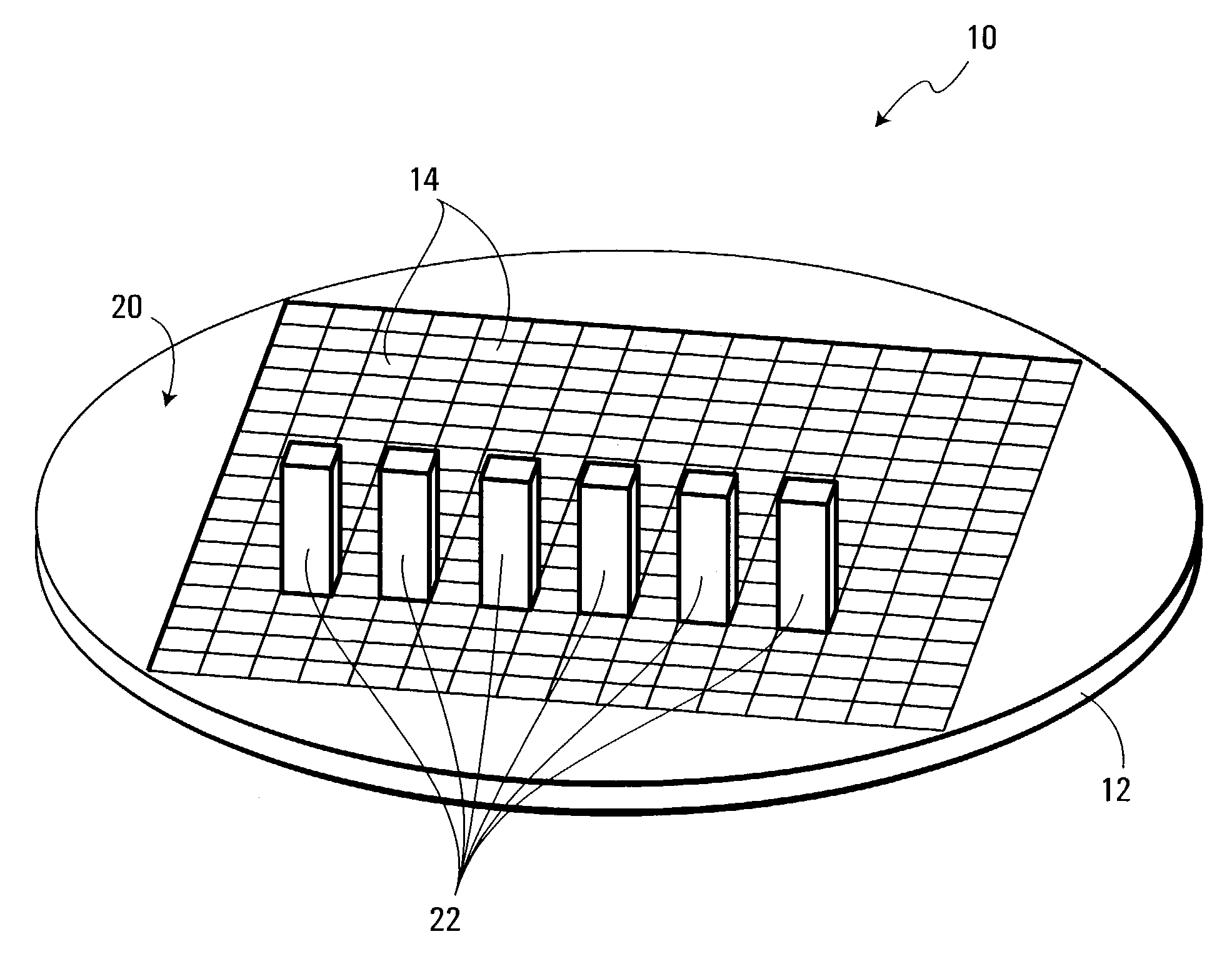
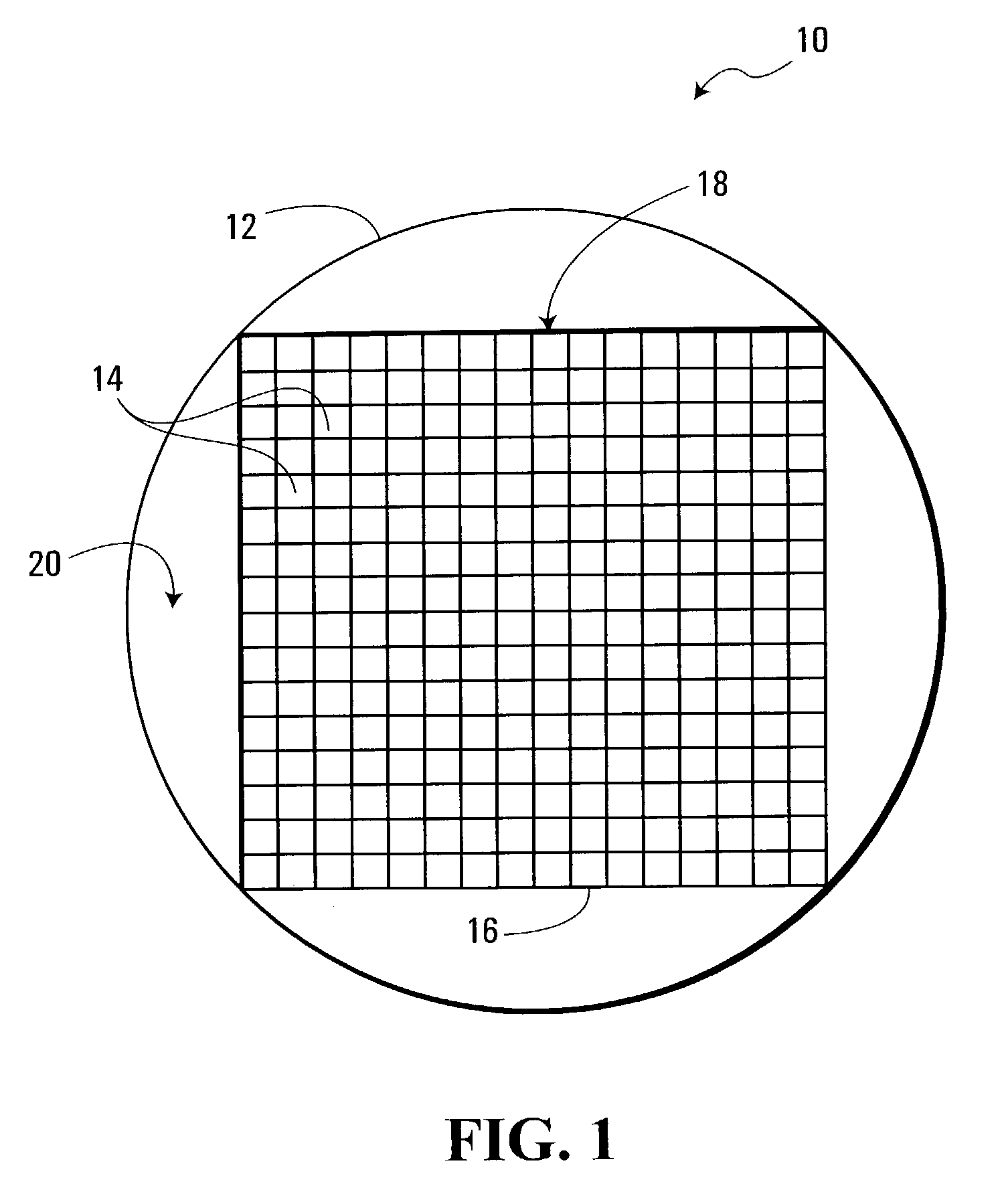
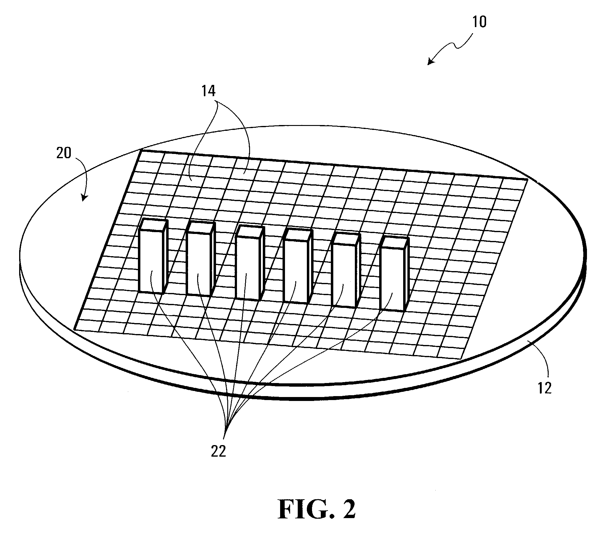
[0030]FIG. 1 is a top view of a semiconductor wafer 10, one example of a typical microelectronic complex. The wafer 10 is formed of a planar body of semiconductor material 12 and contains a plurality of discrete functional modules 14, also referred to as cells. In this particular example of a microelectronic complex, each discrete functional module 14 includes at least one integrated circuit.
[0031]Note that in other examples of microelectronic complexes, such as the integrated circuit itself, the discrete functional modules of the microelectronic complex include the electronic components of the integrated circuit. Further, although the following example of implementation describes a microelectronic complex formed on a semiconductor wafer, the present invention is generally applicable to all microelectronic complexes formed on planar bodies or substrates, or on bodies / substrates defining at least one planar surface, where these bodies / substrates may be of various types of materials.
[...
PUM
 Abstract
Description
Claims
Application Information
 - R&D Engineer
- R&D Manager
- IP Professional
- Industry Leading Data Capabilities
- Powerful AI technology
- Patent DNA Extraction
Browse by: Latest US Patents, China's latest patents, Technical Efficacy Thesaurus, Application Domain, Technology Topic.
© 2024 PatSnap. All rights reserved.Legal|Privacy policy|Modern Slavery Act Transparency Statement|Sitemap