Method and apparatus for specimen fabrication

a technology of a specimen and a fabrication method, which is applied in the field of methods and apparatus for fabricating specimens, can solve the problems of requiring the skill of a well trained person to fabricate the specimen, unable to help resorting to manual work, and a long time, and the method described above cannot help resorting to manual work, and the fabrication of the specimen cannot help. , to achieve the effect of avoiding the occurrence of adsorption of adsorption, avoiding

Inactive Publication Date: 2006-07-04
HITACHI LTD
View PDF20 Cites 61 Cited by
  • Summary
  • Abstract
  • Description
  • Claims
  • Application Information

AI Technical Summary

Benefits of technology

[0013]It is thus an object of the present invention to provide an improved method for fabrication of a specimen capable of solving the problems encountered in the conventional methods described above and to provide a good apparatus for fabrication of a specimen used for implementing the improved specimen fabrication method.
[0014]To be more specific, it is a first object of the present invention to provide a specimen fabrication method capable of fabricating a specimen of a small area to undergo an observation or a measurement / analysis carried out by an observation apparatus such as a TEM or a measurement / analysis apparatus to which the specimen is to be transferred without the need for a well trained person to do manual work such as grinding and dicing and the need to split a semiconductor wafer or an LSI chip by cleaving or cutting.
[0016]It is a third object of the present invention to provide a TEM-specimen holder which is used in conjunction with a TEM and allows a micro-specimen extracted from a specimen substrate to be positioned with ease.
[0037]The micro-specimen separating means has a configuration including an ion-beam irradiating optical system for irradiating an ion beam to the specimen substrate. The ion-beam irradiating optical system is typically a PJIB (projection ion beam) irradiating optical system comprising an ion source and a projection optical system for projecting ions emitted from the ion source on the specimen substrate as a PJIB. As an alternative, the ion-beam irradiating optical system can be an FIB (focused ion beam) irradiating optical system comprising an ion source and a focusing optical system for irradiating ions emitted from the ion source on the specimen substrate as an FIB. As another alternative, the ion-beam irradiating optical system can be a combination of the PJIB irradiating optical system and the FIB irradiating optical system. By irradiation of an ion beam which can be a PJIB or an FIB to the specimen substrate by means of the ion-beam irradiating optical system, the specimen substrate is subjected to sputter fabrication allowing the micro-specimen to be extracted and separated from the specimen surface. In addition, the micro-specimen separating means can also be configured to include a first ion-beam irradiating optical system for irradiating an ion beam to the specimen substrate from a first direction and a second ion-beam irradiating optical system for irradiating an ion beam to the specimen substrate from a second direction different from the first direction. By providing the two ion-beam irradiating optical systems in this way, the process to extract a micro-specimen from the specimen substrate can be carried out more easily. It should be noted that, as the micro-specimen separating means, a laser-beam irradiating optical system or a combination of an ion-beam irradiating optical system and a laser-beam irradiating optical system can also be used as well.
[0041]The specimen fabrication apparatus provided by the present invention may include an observation unit for observing the surface of the specimen substrate, the tip of the probe or the vicinity of the TEM-specimen holder. The observation unit typically comprises an electron-beam irradiating optical system for irradiating an electron beam to the aforementioned member to be observed, a secondary-electron detector for detecting secondary electrons emitted by the observed member due irradiation of the electron beam and a display sub-unit for displaying a secondary-electron image of the observed member by using a detection signal output by the secondary-electron detector. As an alternative, the observation unit can also be implemented by an optical observation apparatus such as an optical microscope. By observing the member to be observed using the observation unit, it is possible to obtain information on a contact / connection state between the tip of the probe and the surface of the specimen substrate, a separation state of the micro-specimen from the surface of the specimen substrate and a contact / connection state between the micro-specimen and the TEM-specimen holder.
[0042]In addition, the specimen fabrication apparatus provided by the present invention may also be provided with a detector for detecting a contact / connection state as well as a separation state between the tip of the probe and the surface of the specimen substrate, between the micro-specimen and the specimen substrate and between the micro-specimen and the TEM-specimen holder. The detector can make use of variations in contact resistance between the members brought into contact with each other or variations in voltage contrast on the secondary-electron image mentioned above. By virtue of the detector, it is possible to obtain information on the contact / connection state and the separation state between the respective members with a high degree of accuracy.

Problems solved by technology

Traditionally, however, fabrication of a specimen for an observation using a TEM can not help resorting to manual work which must be done by a well trained person and takes a long time.
The first and second conventional methods described above can not help resorting to manual work requiring skills of a well trained person fabricating the specimen.
In order to acquire a specimen of a desired area, portions adjacent to the desired area are inevitably and / or inadvertently cleaved or cut.
Since the substrate of the specimen was once cut in order to fabricate specimens for the prior observation and / or analysis, an injury and / or a damage was inevitably and / or inadvertently inflicted upon the portion subjected to the next observation and / or analysis or a positional relation among portions to be observed and / or analyzed is no longer known.
As a result, there is raised a problem that accurate information on observations and / or analyses can not be obtained continuously due to the inflicted injury and / or damage.
In addition, while the ion milling and the process to thin a film by using an FIB described above do not directly involve manual work, they have a problem of a long fabrication time which is difficult to solve.
As a result, splitting a wafer into portions by cleaving or cutting the wafer in order to observe and / or analyze a particular area leads to a disposal to discard portions other the area to be observed and / or analyzed which is very uneconomical.
Otherwise, a number of defective devices among final products will be resulted in, incurring an even larger loss.
In this method, however, the separated specimen remains in a state of being attached to the tip of a probe so that, when the separated specimen is brought into an observation apparatus and / or an analyzer in such a state to be observed and / or analyzed, the specimen will vibrate, raising a problem that it is impossible to obtain reliable results of observation and / or analysis.

Method used


Image

  • Method and apparatus for specimen fabrication
  • Method and apparatus for specimen fabrication
  • Method and apparatus for specimen fabrication

Examples


first embodiment

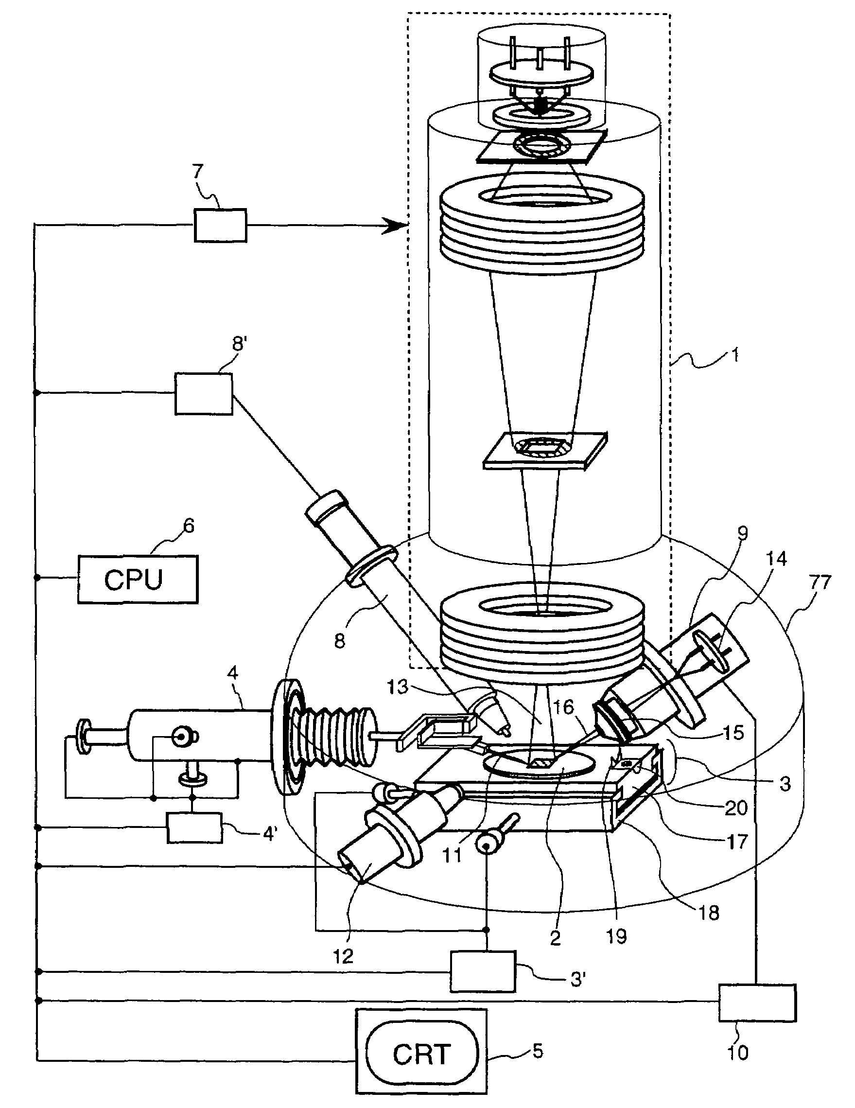
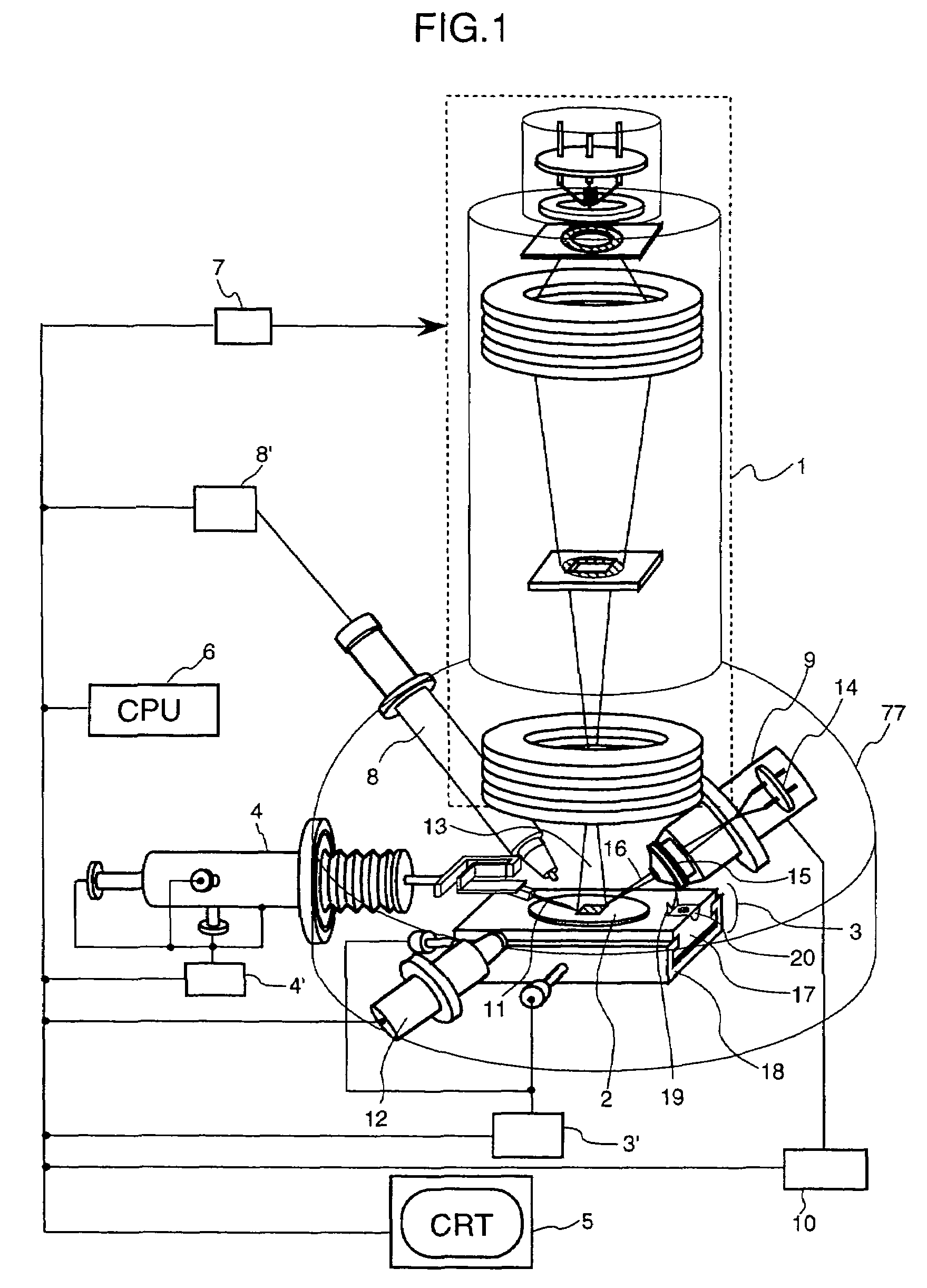
[0077]FIG. 1 is a diagram showing the basic configuration of a specimen fabrication apparatus as implemented by an embodiment of the present invention.

[0078]As shown in the figure, the specimen fabrication apparatus implemented by the embodiment of the present invention comprises:

[0079]an ion-beam irradiating optical system 1 for irradiating an ion beam 13 to a specimen substrate 2 of a specimen, that is, an object of observation, such as a semiconductor wafer or a semiconductor chip;

[0080]a sample stage 3 for moving the specimen substrate 2 mounted thereon;

[0081]a sample-stage position controller 3′ for controlling the position of the sample stage 3 in order to identify a portion of the specimen substrate 2 to be observed or an area to be observed;

[0082]a probe driver 4 for holding and moving a probe 11;

[0083]a probe-driver controller 4′ for controlling the probe driver 4;

[0084]a deposition-gas supplying source 8 for supplying deposition gas, that is, gas used for deposition, to th...

second embodiment

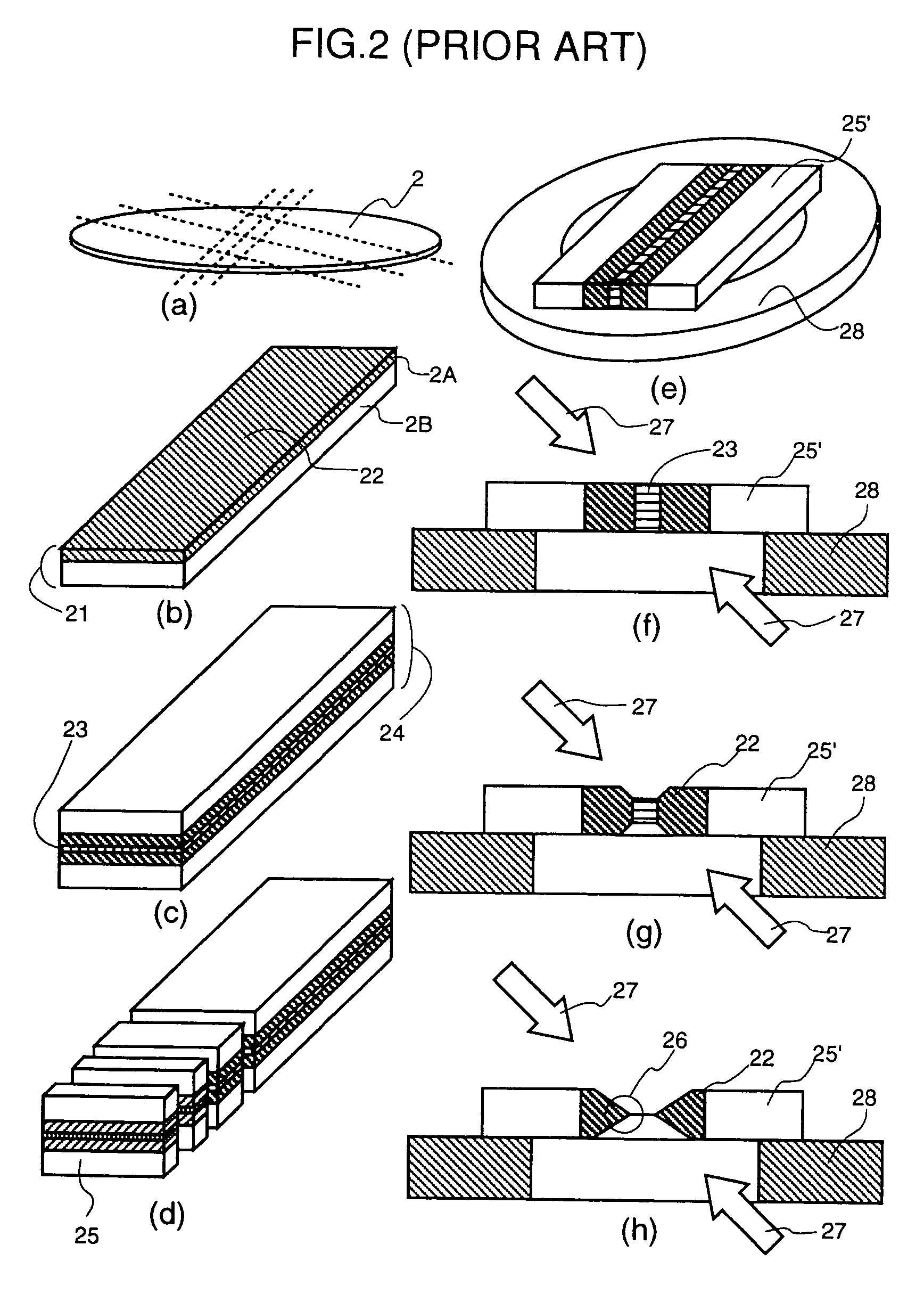
[0133]FIG. 17 is process explanatory diagrams showing another embodiment of the present invention for implementing a method for fabrication of a TEM specimen. The method is adopted in the specimen fabrication apparatus shown in FIG. 1 and only a PJIB is used as an ion beam for fabrication.

[0134]First of all, a PJIB 13′ is irradiated to regions surrounding an observation area 103 on the specimen substrate 2 shown in FIG. 17 / (a) by using a mask with a shape resembling a symbol ‘]’ as shown in FIG. 17 / (b) to form a trench 104 having a bottom with a shape resembling the ‘]’ symbol as shown in FIG. 17 / (c). Then, the sample stage 3 shown in FIG. 1 is inclined to carry out a bottom-dividing fabrication by means of the PJIB 13′ as shown in FIG. 17 / (d). Subsequently, the tip of the probe 11 held by the probe driver 4 is brought into contact with a micro-specimen formation portion 99. The state of contact between the tip of the probe 11 and the micro-specimen formation portion 99 can be verif...

third embodiment

[0137]FIG. 18 is process explanatory diagrams showing a further other embodiment of the present invention for implementing a method for fabrication of a TEM specimen. In this embodiment, a marking process for clarifying a specific position 105 on a micro-specimen 40 to be observed or analyzed is added to the methods for fabrication the micro-specimen 40 described earlier. It should be noted that, since the other processes in this third embodiment are virtually the same as those shown in FIG. 17, their explanation with reference to diagrams is not repeated. In this embodiment, in order to avoid the observation location 105 from being no longer unidentifiable after the micro-specimen 40 including a specific location 105 to be observed has been extracted from the specimen substrate 2, a process to put a mark on the observation location 105 is added in order to clearly show the observation location 105. The observation location 105 is a specific location at which a thin wall portion for...


PUM

PropertyMeasurementUnit
thicknessaaaaaaaaaa
thicknessaaaaaaaaaa
thicknessaaaaaaaaaa

Abstract

A specimen fabrication apparatus including a movable sample stage on which a specimen substrate is mounted, a probe connector for firmly joining a tip of a probe to a portion of the specimen substrate in a vicinity of an area on the specimen substrate to be observed in an observation apparatus, a micro-specimen separator for separating from the specimen substrate a micro-specimen to which the tip of the probe is firmly joined, the micro-specimen including the area on the specimen substrate to be observed and the portion of the specimen substrate to which the tip of the probe is firmly joined, a micro-specimen fixer for fixing the micro-specimen separated from the specimen substrate to a specimen holder of the observation apparatus, and a probe separator for separating the tip of the probe from the micro-specimen fixed to the specimen holder.

Description

CROSS-REFERENCE TO RELATED APPLICATIONS[0001]This is a continuation of U.S. application Ser. No. 10 / 395,237 filed 25 Mar. 2003, now U.S. Pat. No. 6,828,566, which is a division of U.S. application Ser. No. 09 / 202,540 filed 16 Dec. 1998 and issued as U.S. Pat. No. 6,538,254 B1.BACKGROUND OF THE INVENTION[0002]1. Field of the Invention[0003]The present invention relates to a method and an apparatus for fabrication of a specimen. More particularly, the present invention relates to a method and an apparatus for extracting a micro-specimen including a specific small area of a semiconductor material such as a semiconductor wafer or a semiconductor device chip from the semiconductor material by separation using an ion beam and for fabricating a specimen used for carrying out an observation, an analysis and / or a measurement of the specific small area.[0004]2. Description of the Prior Art[0005]In recent years, efforts made to shrink geometries of semiconductor devices make progress at a very...

Claims


Application Information

Patent Timeline
Patent Type & Authority Patents(United States)
IPC IPC(8): H01J37/20G01N1/02G01N1/04G01N1/28G01Q20/00H01J37/305
CPCG01N1/28G01N1/32H01J37/20H01J37/3056H01J37/302G01N2001/028G01N2001/045G01N2001/282H01J2237/31749H01J2237/2007H01J2237/201H01J2237/202H01J2237/31732H01J2237/31745
Inventor TOMIMATSU, SATOSHIUMEMURA, KAORUMADOKORO, YUICHIKAWANAMI, YOSHIMIDOI, YASUNORI
Owner HITACHI LTD
Why Eureka
Try Eureka